Metal base transistor and oscillator using the same

a technology of metal base transistors and oscillators, applied in transistors, electrical devices, semiconductor devices, etc., can solve the problems of inability to achieve several thz as a maximum oscillation frequency required for a thz band spectroscopic instrument, and the cutoff frequency thereof is relatively low, so as to improve the electron velocity of the depletion layer

Inactive Publication Date: 2006-07-27
HITACHI LTD
View PDF0 Cites 2 Cited by
  • Summary
  • Abstract
  • Description
  • Claims
  • Application Information

AI Technical Summary

Benefits of technology

[0011] A conventional MBT has a problem in that a cutoff frequency thereof is relatively low. A principal factor thereof is that a depletion layer electron velocity in a collector composed of WO3 is as low as the order of 106 cm/s. Such a value of the velocity makes the cutoff frequency of the

Problems solved by technology

A conventional MBT has a problem in that a cutoff frequency thereof is relatively low.
As a result, several

Method used


Image

  • Metal base transistor and oscillator using the same
  • Metal base transistor and oscillator using the same
  • Metal base transistor and oscillator using the same

Examples


first embodiment

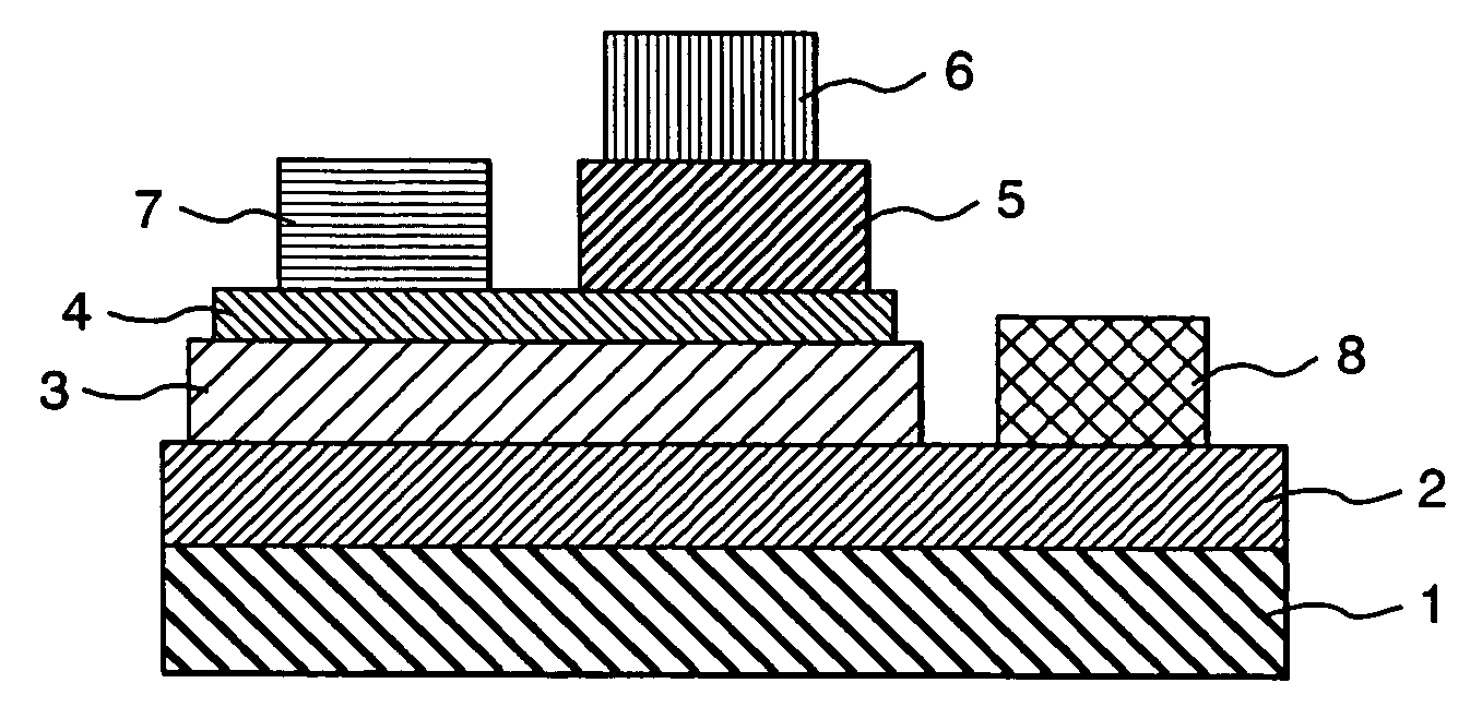
[0048]FIG. 1 is a longitudinal sectional view of an MBT according to a first embodiment of the present invention. The present embodiment employs an emitter-top configuration. Further, the present embodiment employs, for a collector, InN which is a material having an extremely high saturation velocity of electrons.

[0049] A layered mesa structure comprising a high concentration n-type doped InN subcollector layer (electron concentration: 5×1018 cm−3, thickness: 500 nm) 2, an n-type InN collector layer (electron concentration: 5×1016 cm−3, thickness: 500 nm) 3, an Al base layer (thickness: 5 nm) 4 and an Al2O3 emitter layer (thickness: 5 nm) 5 is formed on a sapphire substrate 1. In this mesa structure, an emitter electrode 6, a base electrode 7 and a collector electrode 8 each comprising Au / Pt / Ti are further formed on the emitter layer 5, the base layer 4 and the subcollector layer 2, respectively.

[0050] The present embodiment employs the emitter-top configuration in place of a conv...

second embodiment

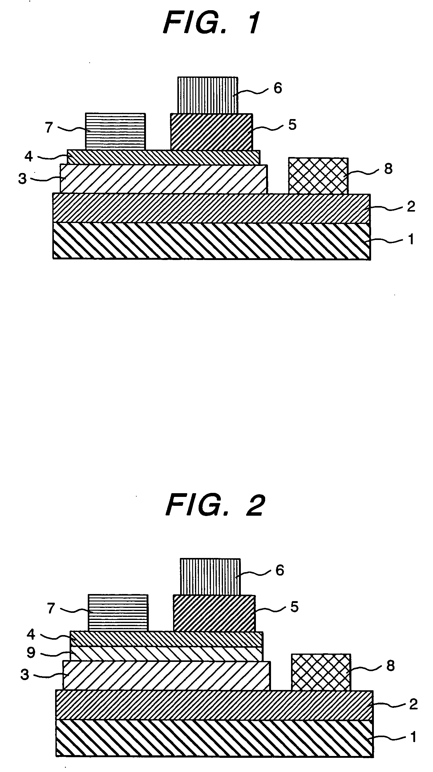
[0053]FIG. 2 is a longitudinal sectional view of the MBT according to a second embodiment of the present invention. As an intermediate layer 9, n-type InGaN having an InN mole fraction of less than 0.5 or p-type InGaN (thickness: 5 nm) having an InN mole fraction of 0.5 or more is inserted between the n-type InN collector layer 3 and Al base layer 4 of the first embodiment. Semiconductor layers other than the layer 9 are the same as those of the first embodiment.

[0054] The first embodiment has a problem in that depending on a formation method of the InN layer, electrons are accumulated in the interface between the collector layer and the metal base layer, and as a result, defects are found in diode operations in base-collector junction. This phenomenon is probably peculiar to materials containing plenty of In such as InN or InAs. On the other hand, according to the present embodiment, the In content at the interface between the base and the collector is reduced so that the accumula...

third embodiment

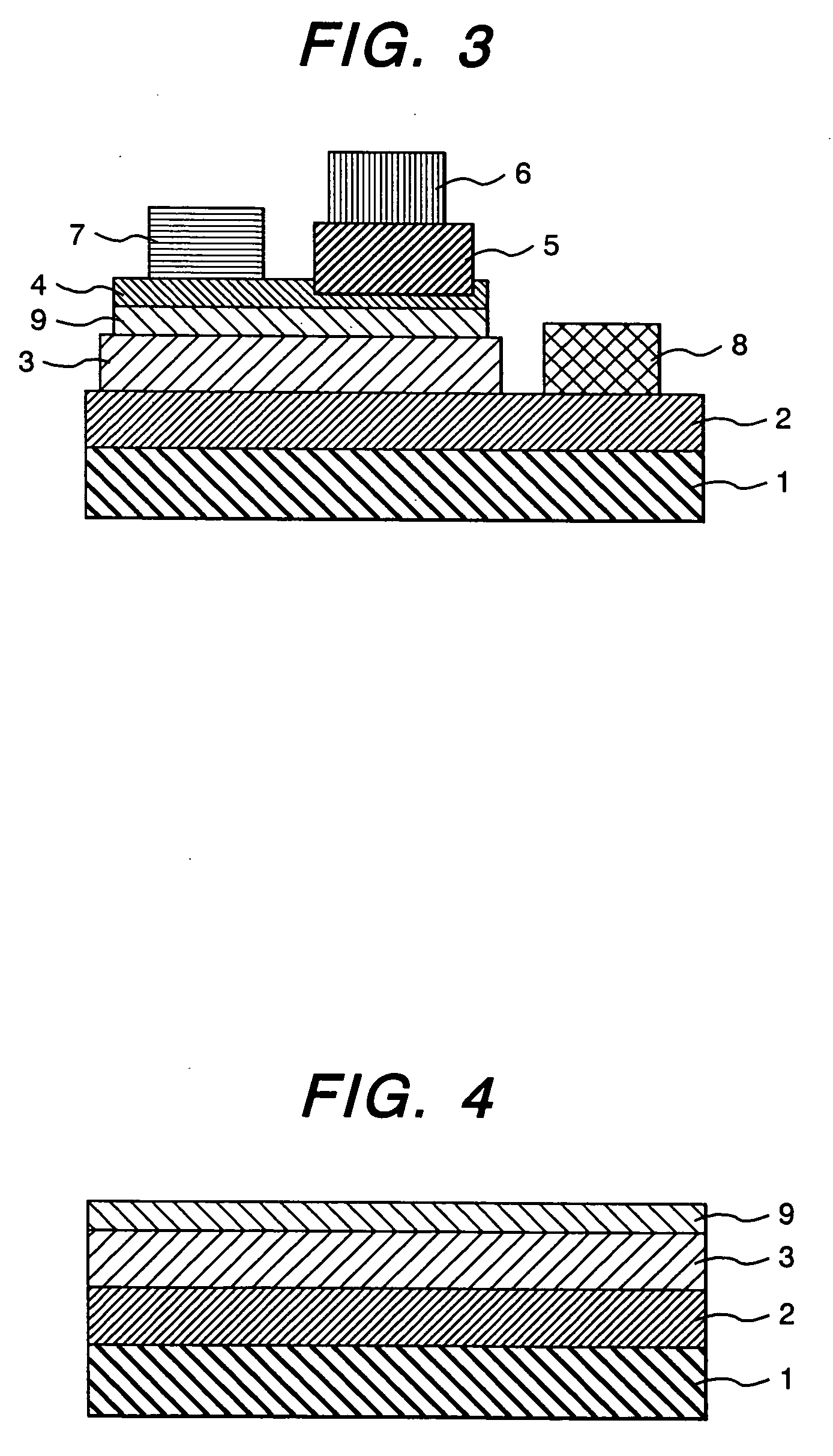
[0056]FIG. 3 is a longitudinal sectional view of the MBT according to a third embodiment of the present invention. A thickness of the base layer 4 in the first or second embodiments is set to 5 nm in the intrinsic region and 10 nm in the extrinsic region. As a result, the maximum oscillation frequency is improved up to 3 THz.

[0057] According to the present embodiment, both of the base transit time and the base resistance can be reduced. As a result, an effect capable of greatly improving the maximum oscillation frequency is obtained.

[0058] In the present embodiment, a thickness in the intrinsic region of the base layer 4 is set to 5 nm; however, the thickness may be set to a value corresponding to one atom layer or more.


PUM


Abstract

The most important task in realizing a downsized and low cost THz band spectroscopic and fluoroscopic instrument is to achieve downsizing and cost reduction of oscillators used in the instrument. A metal base transistor is used for an active element of the oscillator. In order to improve the maximum oscillation frequency of the transistor to several THZ, InN having a high electron saturation velocity or a material mainly composed of InN is used for a collector layer. In order to obtain characteristics with excellent reproducibility, it is useful to insert InGaN into an interface between the collector layer and the base layer. Using the metal base transistor of the present invention makes it possible to constitute an oscillator allowing a THz band oscillation. Further, the present invention provides a spectroscopic instrument applying this oscillator to at least one of a signal source and a local oscillator.

Description

[0001] The present application claims priority from Japanese application JP 2005-017724, filed on Jan. 26, 2005, the content of which is hereby incorporated by reference into this application. BACKGROUND OF THE INVENTION [0002] 1. Field of the Invention [0003] The present invention relates to an ultra-high-speed transistor and an oscillator using the same. [0004] 2. Description of the Related Art [0005] As the needs of dangerous article detection increase, a terahertz (THz) band spectroscopic technique capable of nondestructively identifying a substance attracts attention. Further, the effective utilization of the THz band is already verified by a method of using light for a light source, such as a free electron laser, a p-type germanium laser, light injection type parametric generation and optical mixing on the optical switching. The comparison of these techniques is disclosed, for example, in Japanese Society of Radiological Technology Academic Journal Vol. 58, No. 4 (2002), pp. 4...

Claims


Application Information

Patent Timeline
IPC IPC(8): H01L27/082
CPCH01L29/2003H01L29/7606
Inventor MOCHIZUKI, KAZUHIROTANAKA, SHIGEHISATANOUE, TOMONORI
Owner HITACHI LTD
Why Eureka
Try Eureka