

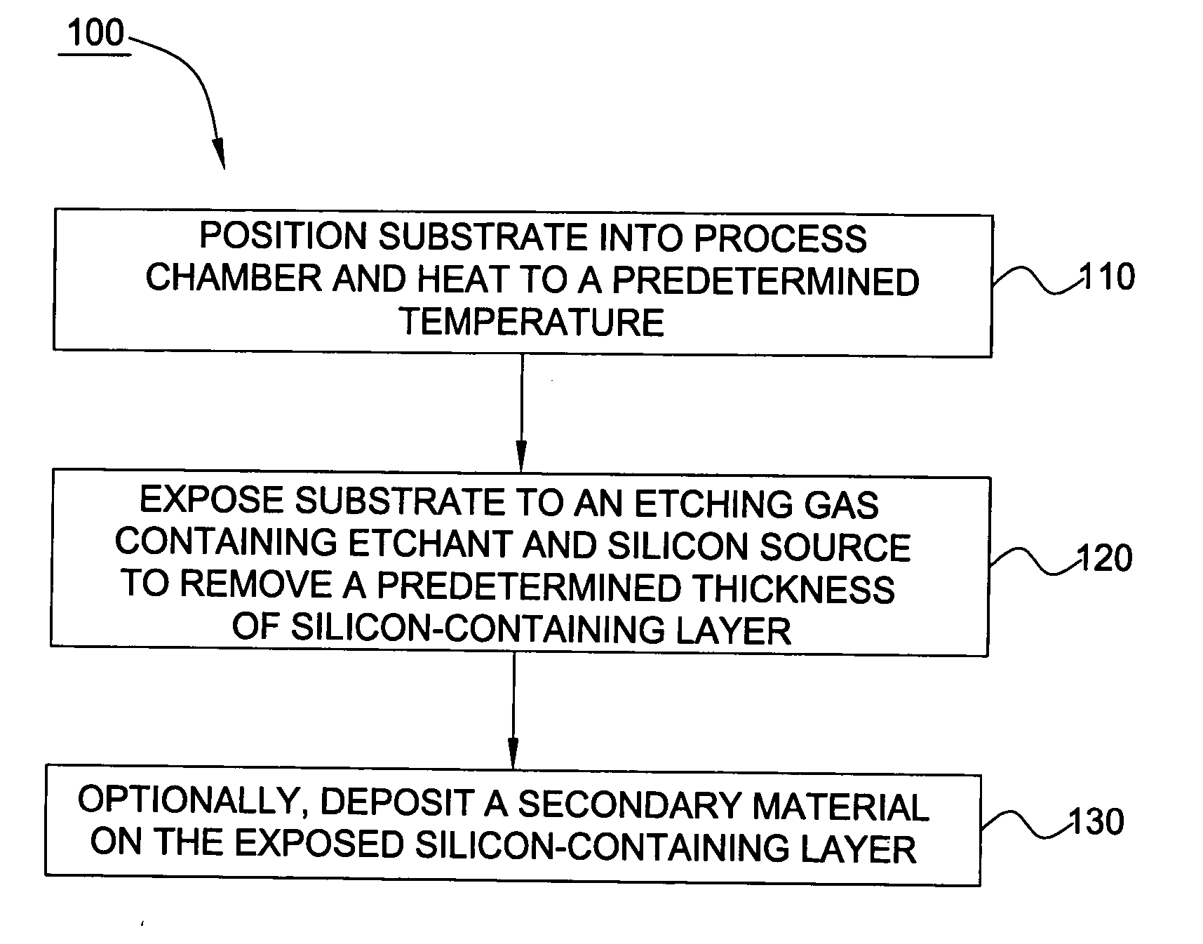
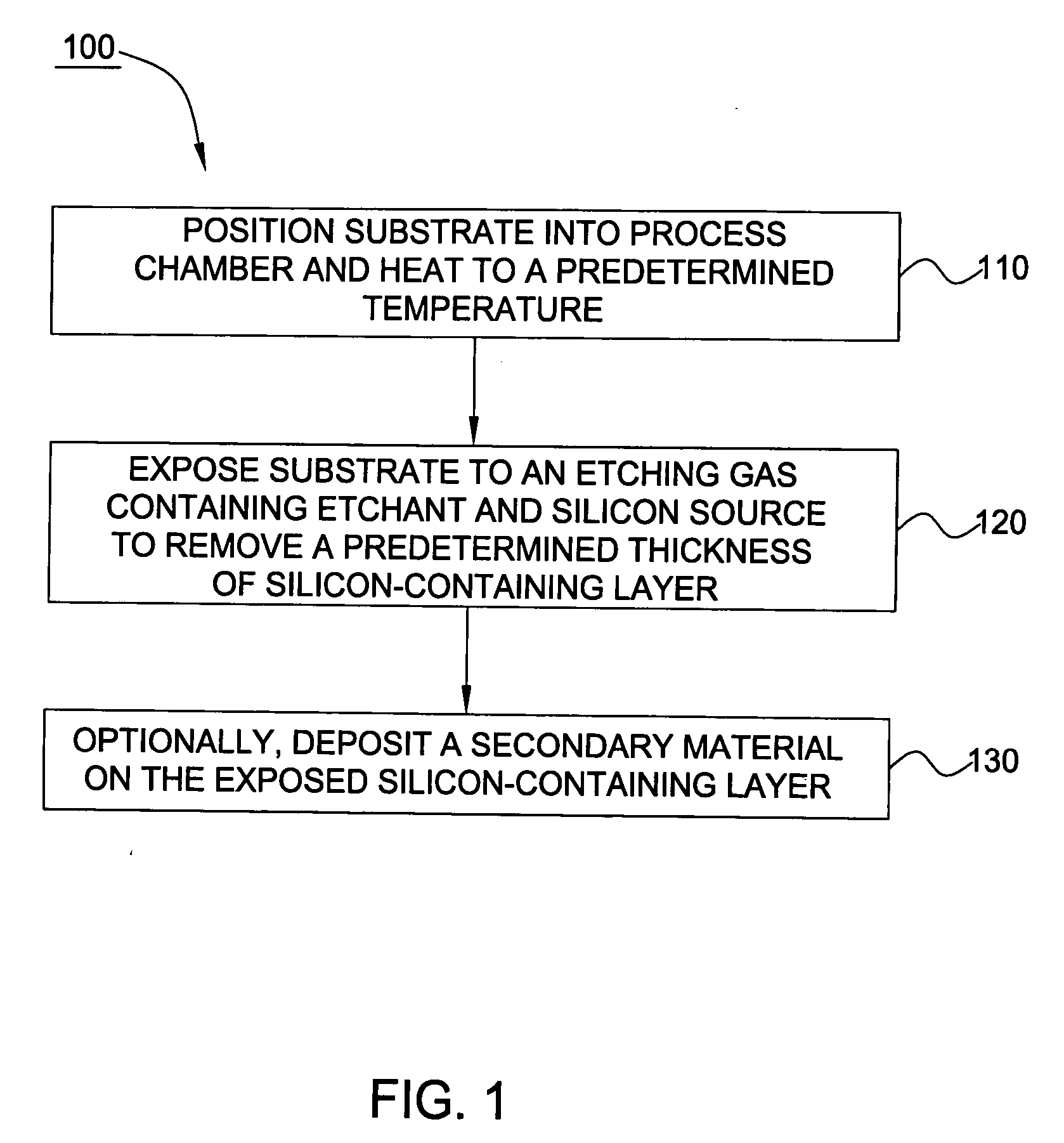
Low temperature etchant for treatment of silicon-containing surfaces
a technology of silicon-containing surfaces and low temperature, applied in electrostatic cleaning, cleaning processes and apparatuses, chemical instruments and processes, etc., can solve the problems of poor device performance and reliability, rough surface containing a silicon-containing material, poor quality interfaces
- Summary
- Abstract
- Description
- Claims
- Application Information
AI Technical Summary
Benefits of technology
Problems solved by technology
Method used
Image

Examples
example 1
Pre-clean Process Comparative Without Silane
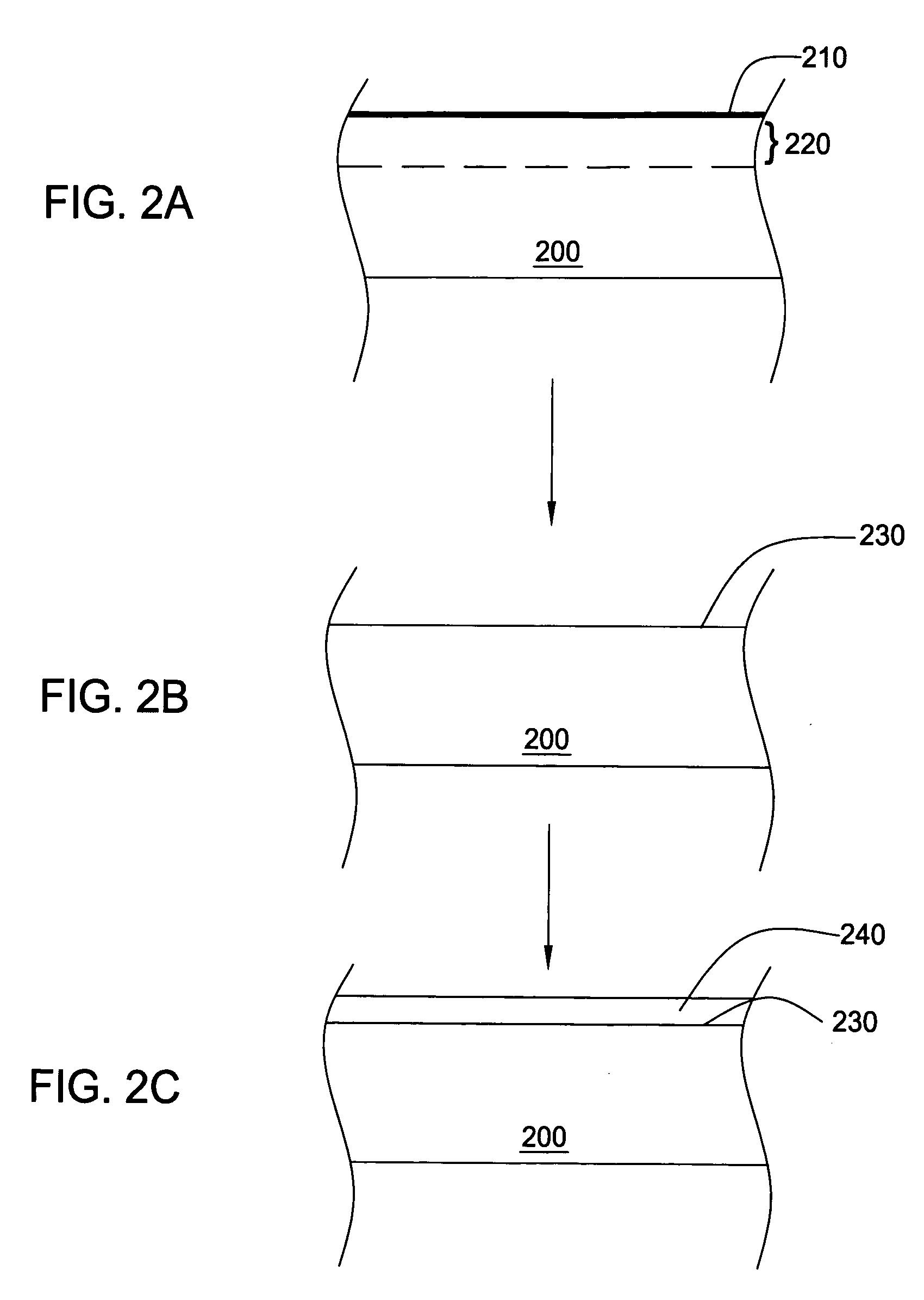
[0058] A substrate was exposed to an HF-last process to form a fluoride terminated surface. The substrate was placed in the process chamber and heated to about 600° C. while the atmosphere was maintained at about 20 Torr. The substrate was exposed to an etching gas containing N2 at a flow rate of about 20 slm and Cl2 at flow rate of about 120 sccm. The surface was etched at a rate of about 500 Å / min.
example 2
Pre-clean Process with Silane
[0059] A substrate was exposed to an HF-last process to form a fluoride terminated surface. The substrate was placed in the process chamber and heated to about 600° C. while the atmosphere was maintained at about 20 Torr. The substrate was exposed to an etching gas containing N2 at a flow rate of about 20 slm, Cl2 at flow rate of about 20 sccm and SiH4 at a flow rate of about 50 sccm. The surface was etched at a rate of about 10 Å / min. Therefore, the addition of a silicon source, such as silane in Example 2, reduced the etch rate of the silicon-containing layer by about 50 times as compared to the etch rate in Example 1.
example 3
Smoothing Process Comparative Without Silane
[0060] A substrate surface containing a silicon-containing layer was cleaved forming a surface with a roughness of about 5.5 nm root mean square (RMS). The substrate was placed in the process chamber and heated to about 650° C. while the atmosphere was maintained at about 200 Torr. The substrate was exposed to an etching gas containing N2 at a flow rate of about 20 slm and Cl2 at flow rate of about 20 sccm. The surface was etched at a rate of about 200 Å / min.
PUM
| Property | Measurement | Unit |
|---|---|---|
| Temperature | aaaaa | aaaaa |
| Temperature | aaaaa | aaaaa |
| Time | aaaaa | aaaaa |
Abstract
Description
Claims
Application Information