Film pattern forming method, film pattern, resist film, insulation film, circuit board, semiconductor device, surface elastic wave device, surface elastic wave oscillation device, electro-optic device, and electronic device

a film pattern and film pattern technology, applied in the direction of printed circuit manufacturing, printed circuit aspects, semiconductor devices, etc., can solve the problems of increasing the surface area necessary to form the film pattern, the droplet shape cannot be maintained, and the droplet wet-spreading of the margin part of the margin area is difficult to achieve, so as to reduce the outward direction of wet-spreading of the droplet, the effect of increasing the thickness and reducing the flow

Inactive Publication Date: 2006-08-03
SEIKO EPSON CORP
View PDF4 Cites 10 Cited by
  • Summary
  • Abstract
  • Description
  • Claims
  • Application Information

AI Technical Summary

Benefits of technology

[0007] An advantage of the present invention is to provide a film pattern forming method, film pattern, resist film, insulation film, and circuit board, semiconductor device, surface elastic wave device, surface elastic wave oscillation device, electro-optic device, and electronic device, which are capable of restricting the applied liquid material from flowing from the film pattern forming region and from wetting outside the film pattern forming region so as to be able to form a film pattern having a predetermined pattern shape and thickness without having to require an additional surface area outside the film pattern forming region.
[0008] The film pattern forming method of the present invention is a film pattern forming method for forming a film pattern on a predetermined region of a substrate that has a predetermined shape. The method includes rendering a surface of the substrate liquid-repellent; applying droplets of a liquid containing material for forming the film pattern in a margin area of the predetermined region in which the film pattern is to be formed, thereby forming a margin band of the applied droplets and forming a margin band film by drying or hardening the margin band; rendering the surface of the substrate lyophilic; and applying droplets of the liquid in the predetermined region circumscribed by the margin band film and thereby filling the predetermined region.
[0009] According to the method of this aspect of the present invention, a margin band of droplets is formed in the margin of the predetermined region by the margin forming process, which forms the margin band film. The droplets for forming the margin band are arranged in the margin area of the predetermined region, and spread from the applied positions bi-directionally in the outward direction and inward direction of the margin area. In a method for applying the droplets in which droplets are applied continuously in the entirety of the margin area, since droplets are applied continuously in the margin area and the predetermined region that is connected to the margin area, the droplets arranged in the margi

Problems solved by technology

Since the bank must be arranged so as to circumscribe the film pattern forming region, a problem arises inasmuch as both a film pattern forming region and a bank forming region are required, thus increasing the surface area necessary to form the film pattern.
A further problem arises in that, processes and a manufacturing apparatus for forming the bank are also required in addition to the processes for forming the film pattern itself and the manufacturing apparatus for the film pattern itself.
Furthermore, by treating the substrate surface with a liquid-repellency process before the margin

Method used


Image

  • Film pattern forming method, film pattern, resist film, insulation film, circuit board, semiconductor device, surface elastic wave device, surface elastic wave oscillation device, electro-optic device, and electronic device
  • Film pattern forming method, film pattern, resist film, insulation film, circuit board, semiconductor device, surface elastic wave device, surface elastic wave oscillation device, electro-optic device, and electronic device
  • Film pattern forming method, film pattern, resist film, insulation film, circuit board, semiconductor device, surface elastic wave device, surface elastic wave oscillation device, electro-optic device, and electronic device

Examples


first embodiment

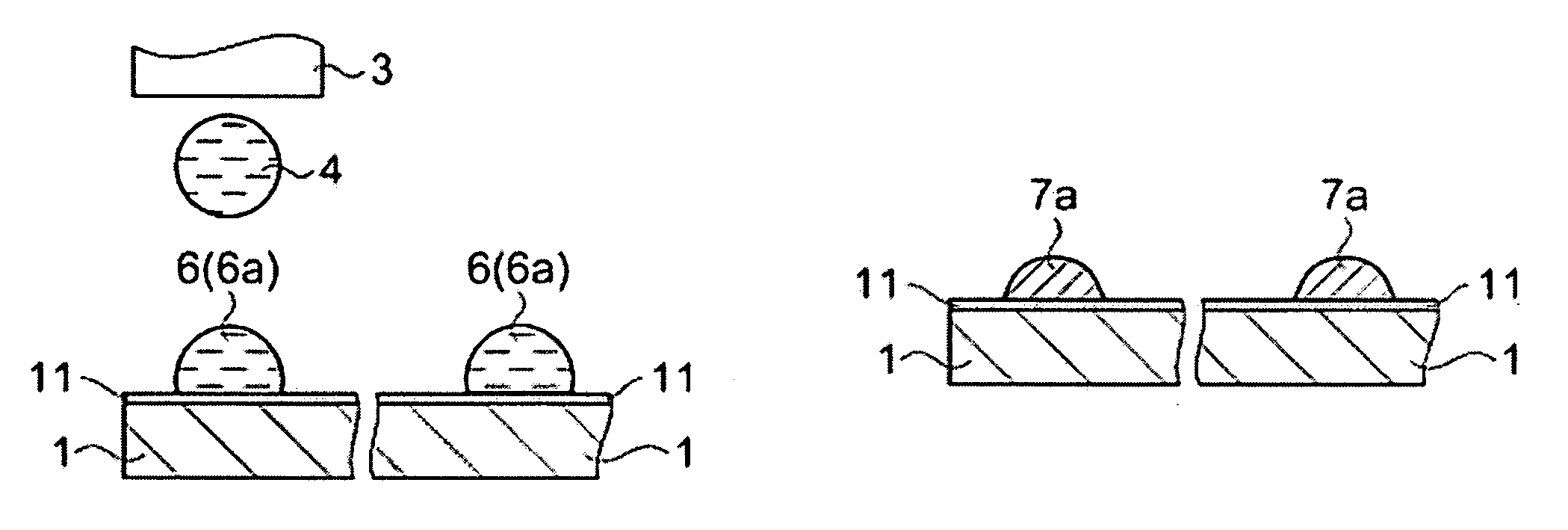
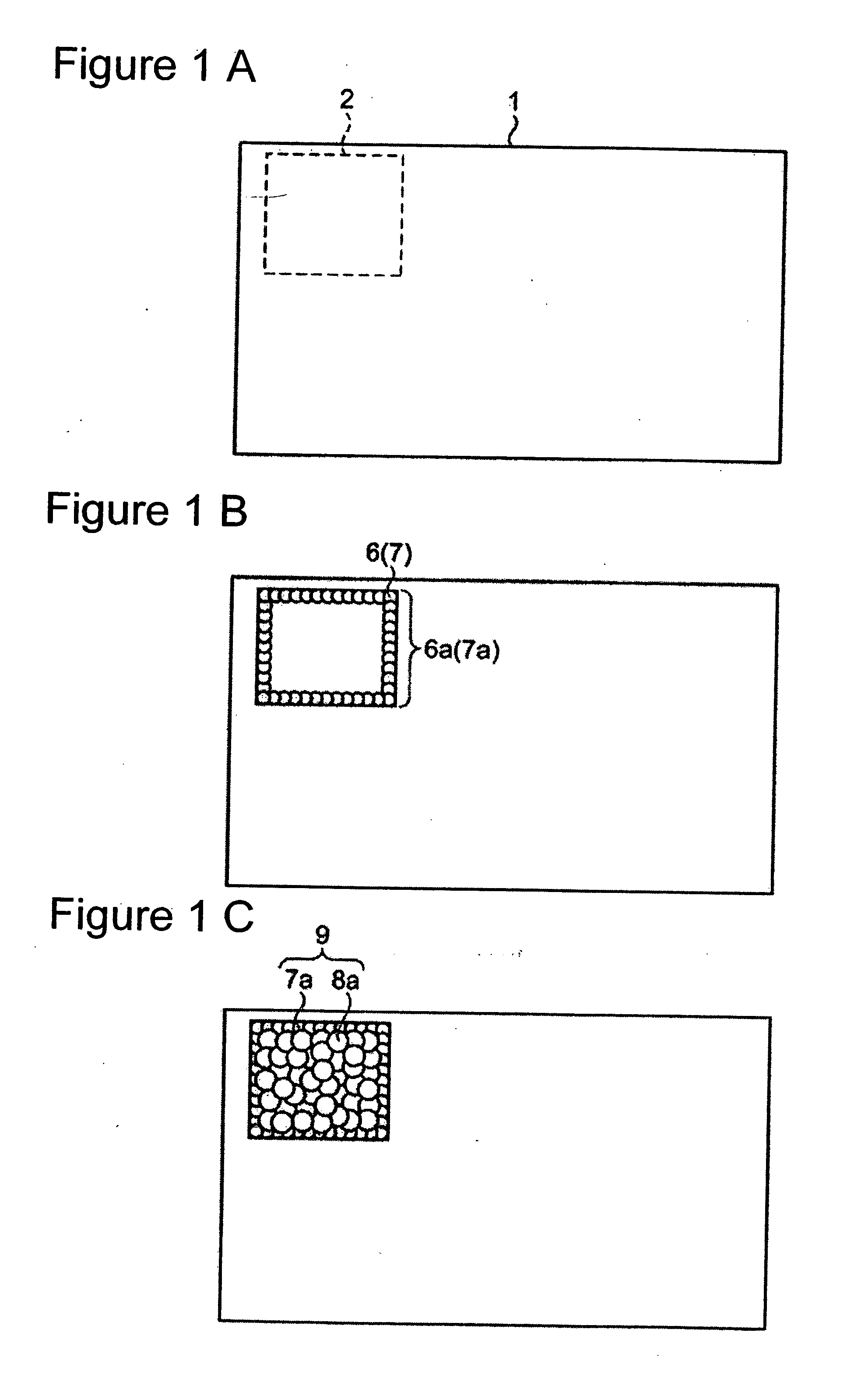
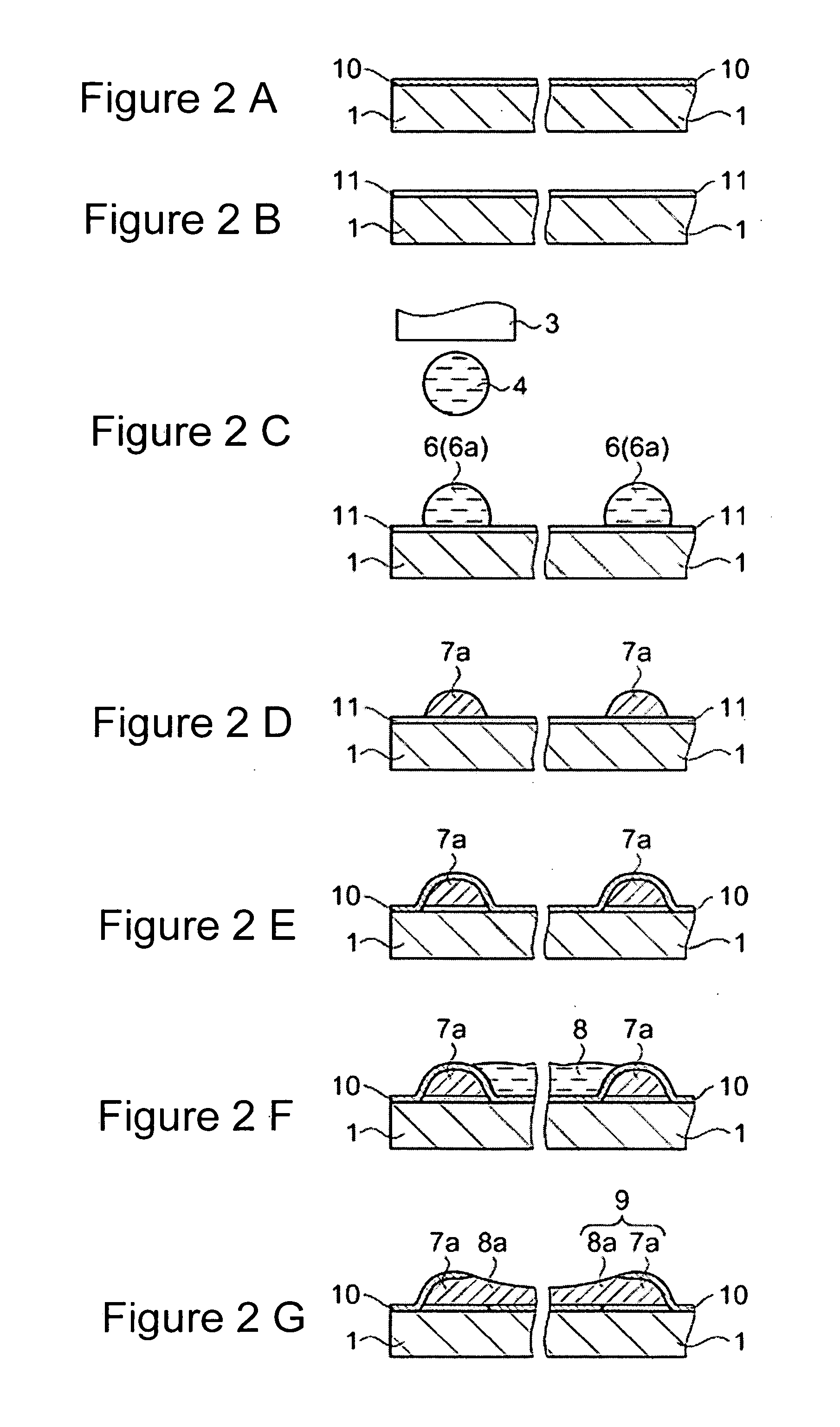
[0098]FIG. 1 is a schematic plan view showing the film pattern forming method of the FIG. 2 is a schematic cross section view showing the film pattern forming method of the present embodiment. A substrate 1 shown in FIG. 1 is a liquid crystal substrate of, for example, a surface elastic wave device. An example is described wherein a resist film 9 is formed in a region 2 indicated by the dashed lines in FIG. 1A. Region 2 corresponds to a margin area, and a resist film 9 corresponds to a resist film and film pattern.

[0099] First, the surface of the substrate 1 is subjected to a lyophilic process to form a lyophilic film 10 on the surface including the region 2, as shown in FIG. 2A. Then, the surface of the substrate 1 is subjected to a liquid repellency process to mitigate lyophilic property of the lyophilic film 10 and form a liquid-repelling film 11, as shown in FIG. 2B. The thickness of the lyophilic film 10 and liquid-repelling film 11 is approximately a one-molecule layer. Next,...

second embodiment

[0184] The second embodiment provides the following effects.

[0185] (1) Droplets of applied liquid etching resist material are prevented from flowing from the electrode forming region and wetting outside the electrode forming region by forming an etching resist film in a predetermined electrode shape and thickness. Accordingly, electrodes such as the IDT 55, reflectors 56a and 56b, and connecting lands 57a and 57b can be formed in precise shapes.

[0186] (2) Applied liquid anodic oxidation resist film material is prevented from flowing outside the connecting lands 57a and 57b forming regions and wetting outside the regions by forming an anodic oxidation resist film of sufficient thickness and accurately covering the connecting lands 57a and 57b. Accordingly, the anodic oxidation resist film covering the connecting lands 57a and 57b can be formed at the connecting lands 57a and 57b without covering the IDT 55 that requires the anodic oxidation process.

[0187] (3) Applied liquid anodic ...

third embodiment

[0206] The third embodiment provides the following effects.

[0207] (1) The liquid insulation film material for forming the fill-in part 91 is prevented from flowing through the through hole 86 by the formation of the hole margin 88. Accordingly, it is possible to form the insulation film directly next to the through hole 86, and the insulation film 92 for covering the circuit lead 83 can be formed without covering the mutually adjacent through hole 86 and through hole 86 in the circuit lead 83.

[0208] (2) The liquid insulation film material for forming the fill-in part 91 is prevented from covering the land 84a by forming the land margin 87. Accordingly, it is possible to form the insulation film directly next to the land 84a, and the insulation film 92 for covering the circuit lead 83 can be formed without covering the mutually adjacent land 84a and land 84a in the circuit lead 83.

[0209] (3) The liquid repellency process is performed before the droplets of liquid insulation materia...


PUM

PropertyMeasurementUnit
Contact angleaaaaaaaaaa
Viscosityaaaaaaaaaa

Abstract

A film pattern forming method is for forming a film pattern on a predetermined region of a substrate that has a predetermined shape. The film pattern forming method includes: rendering a surface of the substrate liquid-repellent; applying droplets of a liquid containing material for forming the film pattern in a margin area of the predetermined region in which the film pattern is to be formed, thereby forming a margin band of the applied droplets and forming a margin band film by drying or hardening the margin band; rendering the surface of the substrate lyophilic; and applying droplets of the liquid in the predetermined region circumscribed by the margin band film and thereby filling the predetermined region.

Description

BACKGROUND [0001] 1. Technical Field [0002] The present invention relates to a film pattern forming method; a film pattern, an insulation film, and a resist film that are manufactured using the film pattern forming method; and a circuit board a semiconductor device, a surface elastic wave device, a surface elastic wave oscillation device, an electro-optic device, and an electronic device that are provided with one of the resist film, the insulation film, and the resist film. [0003] 2. Related Art [0004] Semiconductor devices, circuit boards, surface elastic wave devices and the like, in which a laminated layer of a circuit wiring of a film pattern of a conductive body (hereinafter referred to as “wiring film”) and a film pattern of an insulation film or the like covering the wiring film is formed on a substrate, are known. Furthermore, film patterns such as resist films are known to be formed and used in the processes of manufacturing these devices. So-called inkjet methods, such as...

Claims


Application Information

Patent Timeline
IPC IPC(8): B44C1/22C23F1/00C03C15/00
CPCH05K3/1208H05K3/125H05K3/28H05K2201/09909H05K2203/013H05K2203/1173H05K2203/1476H10K71/135
Inventor TOYODA, NAOYUKI
Owner SEIKO EPSON CORP
Why Eureka
Try Eureka