Electronic device and method for fabricating the same

a technology of electronic devices and fabrication methods, applied in the direction of semiconductor devices, semiconductor/solid-state device details, electrical apparatus, etc., can solve the problems of increasing costs, affecting the thermal expansion coefficient of integrated circuit chips, and affecting the thermal expansion coefficient of saw chips

Inactive Publication Date: 2006-08-03
FUJITSU LTD
View PDF12 Cites 61 Cited by
  • Summary
  • Abstract
  • Description
  • Claims
  • Application Information

AI Technical Summary

Benefits of technology

[0031] Accordingly, sufficient contacdt areas can be obtained beween the first sealing structure and the second sealing structure and between the first electrode and the second electrode. Thus, according t

Problems solved by technology

However, in the conventional methods, the metal cover, the package of ceramics or others are expensive, which increases the cost.
The cover and the package itself are relatively large, which might be a barrier to smaller-sizing the electronic device.
Furthermore, the above-described patent references have the following problem.
However, this structure has a problem that stresses are applied to the SAW chips due to high bonding temperatures of the intermetallic compound.
However, this structure has a problem that the barrier bumps (of solder, gold or others) are melted to be bonded

Method used


Image

  • Electronic device and method for fabricating the same
  • Electronic device and method for fabricating the same
  • Electronic device and method for fabricating the same

Examples


first embodiment

A FIRST EMBODIMENT

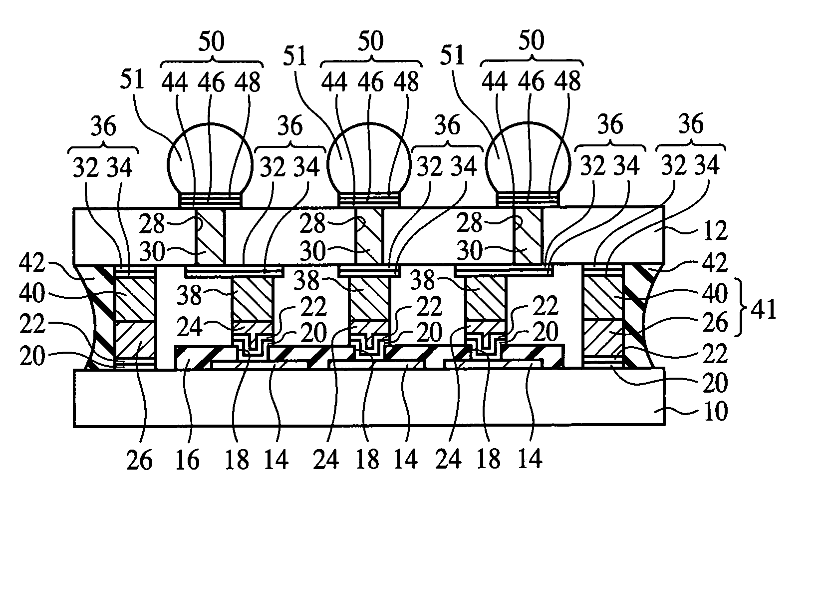
[0055] The electronic device according to a first embodiment of the present invention and the method for fabricating the electronic device will be explained with reference to FIGS. 1 to 13C. FIG. 1 is a sectional view of the electronic device according to the present embodiment.

[0056] (The Electronic Device)

[0057] As illustrated in FIG. 1, the electronic device according to the present embodiment, a semiconductor substrate 10 and a sealing substrate 12 are opposed to each other.

[0058] In predetermined regions of one primary surface of the semiconductor substrate 10, an integrated circuit (not illustrated) including electronic circuit elements (not illustrated) comprising semiconductor elements, such as transistors, etc. is formed.

[0059] That is, in the predetermined regions of one primary surface of the semiconductor substrate 10, active devices, such as transistors, etc. (not illustrated) and / or passive devices, such as capacitors, etc. (not illustrated) are f...

second embodiment

A SECOND EMBODIMENT

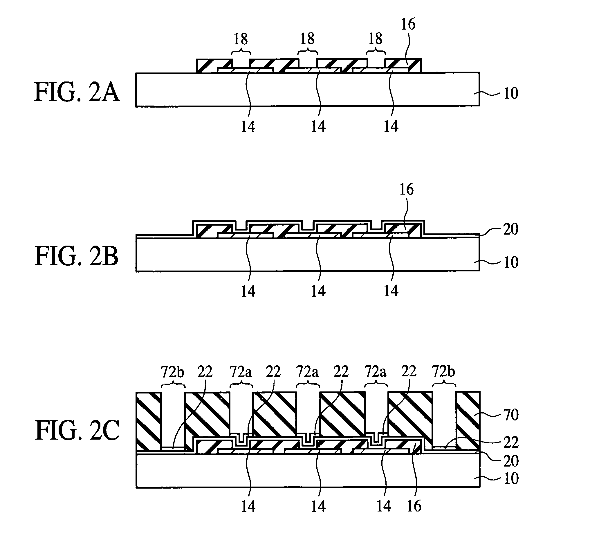
[0239] The method for fabricating the electronic device according to a second embodiment of the present invention will be explained with reference to FIGS. 18A to 20C.

[0240]FIG. 18A to 20C are sectional views of the electronic device according to the present embodiment in the steps of the method for fabricating the electronic device, which illustrate the method.

[0241] The same members of the present embodiment as those of the electronic device according to first embodiment and the method for fabricating the electronic device illustrated in FIGS. 1 to 17C are represented by the same reference numbers not to repeat or to simplify their explanation.

[0242] The method for fabricating the electronic device according to the present embodiment is characterized in that an adhesion layer 42b is formed on the side surface of a sealing structure 40 on the side of a sealing substrate 12, and an adhesion layer 78b is formed on the side surface of a sealing structure 26 on th...

third embodiment

A THIRD EMBODIMENT

[0282] The method for fabricating the electronic device according to a third embodiment of the present invention will be explained with reference to FIGS. 21A to 23C. FIGS. 21A to 23C are sectional views of the electronic device according to the present embodiment in the steps of the method for fabricating the electronic device, which illustrate the method.

[0283] The same members of the present embodiment as those of the electronic device according to the first or the second embodiment and the method for fabricating the electronic device illustrated in FIGS. 1 to 20C are represented by the same reference numbers not to repeat or to simplify their explanation.

[0284] The method for fabricating the electronic device according to the present embodiment is characterized in that no adhesion layer is formed on the side of a sealing substrate 12, and an adhesion layer is formed only on the side of a semiconductor substrate 10.

[0285] First, the step of preparing the semi...


PUM


Abstract

The electronic device comprises a first substrate 10 with an electric circuit element formed in a predetermined region of one primary surface, a second substrate 12 formed, opposed to said one primary surface of the first substrate 10, sealing portions 26, 40 formed between the first substrate 10 and the second substrate 12, enclosing the predetermined region of the first substrate 10, and an adhesion layer 42 formed on the side surfaces of the sealing parts 26, 40. The adhesion layer is formed on the side surfaces of the first sealing structure 26 on the side of the first substrate 10 and the second sealing structure 40 on the side of the second substrate 12, whereby when the first sealing structure 26 and the second sealing structure 40 are bonded to each other, the adhesion between the first sealing structure 26 and the second sealing structure 40 can be sufficiently ensured.

Description

CROSS-REFERENCE TO RELATED APPLICATION [0001] This application is based upon and claims priority of Japanese Patent Application No. 2005-22694, filed on Jan. 31, 2005, the contents being incorporated herein by reference. BACKGROUND OF THE INVENTION [0002] The present invention relates to an electronic device and a method for fabricating the electronic device, more specifically, an electronic device having electronic circuit elements hermetic sealed and a method for fabricating the electronic device. [0003] As electronic circuit elements are increasingly highly integrated by the progress of the recent micronization technology, drastic increase of the processing speed and the cost reduction have been realized. [0004] Semiconductor devices for industrial apparatuses, and cars are considered to be used in severe environments, as of high temperature, high humidity, etc. The semiconductor chips must be sealed in a package having high sealing performance. [0005] SAW (Surface Acoustic Wave)...

Claims


Application Information

Patent Timeline
IPC IPC(8): H01L23/02
CPCH01L23/041H01L23/10H01L23/3114H01L23/49827H01L24/11H01L24/12H01L24/16H01L24/31H01L24/81H01L2224/0401H01L2224/0603H01L2224/1147H01L2224/13099H01L2224/13144H01L2224/13147H01L2224/1403H01L2224/16H01L2224/81193H01L2224/81194H01L2224/81203H01L2224/81801H01L2224/83907H01L2224/83951H01L2924/01002H01L2924/01005H01L2924/01013H01L2924/01022H01L2924/01027H01L2924/01029H01L2924/0105H01L2924/01075H01L2924/01078H01L2924/01079H01L2924/01327H01L2924/09701H01L2924/14H01L2924/15311H01L2924/19041H03H9/059H01L2224/13111H01L2924/01006H01L2924/01019H01L2924/01033H01L2924/014H01L2224/8183H01L2224/06102H01L24/13H01L24/27H01L24/29H01L24/32H01L24/73H01L24/83H01L2224/05124H01L2224/05147H01L2224/05166H01L2224/05655H01L2224/06051H01L2224/0615H01L2224/1184H01L2224/14H01L2224/16238H01L2224/29011H01L2224/73103H01L2224/73203H01L2224/8182H01L2224/8382H01L2224/9211H01L2924/15787H01L2924/15788H01L2924/00H01L2924/00014
Inventor MIZUKOSHI, MASATAKA
Owner FUJITSU LTD
Why Eureka
Try Eureka