Bump structure of semiconductor device and method of manufacturing the same

a semiconductor device and bump technology, applied in semiconductor devices, semiconductor/solid-state device details, electrical devices, etc., can solve problems such as reducing reducing the reliability of the device, and affecting the performance of the device, so as to achieve the effect of increasing the bonding force of the bump in the semiconductor packag

Inactive Publication Date: 2006-08-03
SAMSUNG ELECTRONICS CO LTD
View PDF9 Cites 28 Cited by
  • Summary
  • Abstract
  • Description
  • Claims
  • Application Information

AI Technical Summary

Benefits of technology

[0031] In accordance with the present invention, the bonding force of a bump in a semiconductor package can be increased, and an under cut that otherwise is formed in a UBM can be prevented.

Problems solved by technology

As the height, or bonding surface area, of a bump is decreased to conform with such height restrictions, device reliability is degraded.
Also, when etching an Under Bump Metal (UBM) mounted as a lower layer of the bump after forming the bump, an undesirable under cut may occur.
Such an under cut of the UBM is regarded as lowering the bonding force of the bump and degrading electrical reliability of the bump.
The decreased bonding force of the bump 50 causes a significant problem if a smaller bump size or bump pad pitch is required.
However, if the height of the bump 50, for example the height of the FIG. 1 bump structure, is reduced, the reliability to the bump is likely to become degraded.
Therefore, the restriction in the decrease of the bump thickness operates as a final factor that impedes further reduction of the package thickness.

Method used


Image

  • Bump structure of semiconductor device and method of manufacturing the same
  • Bump structure of semiconductor device and method of manufacturing the same
  • Bump structure of semiconductor device and method of manufacturing the same

Examples


first embodiment

[0039]FIGS. 2 through 6 are sectional views illustrating a bump of the semiconductor device and a manufacturing method thereof according to the present invention.

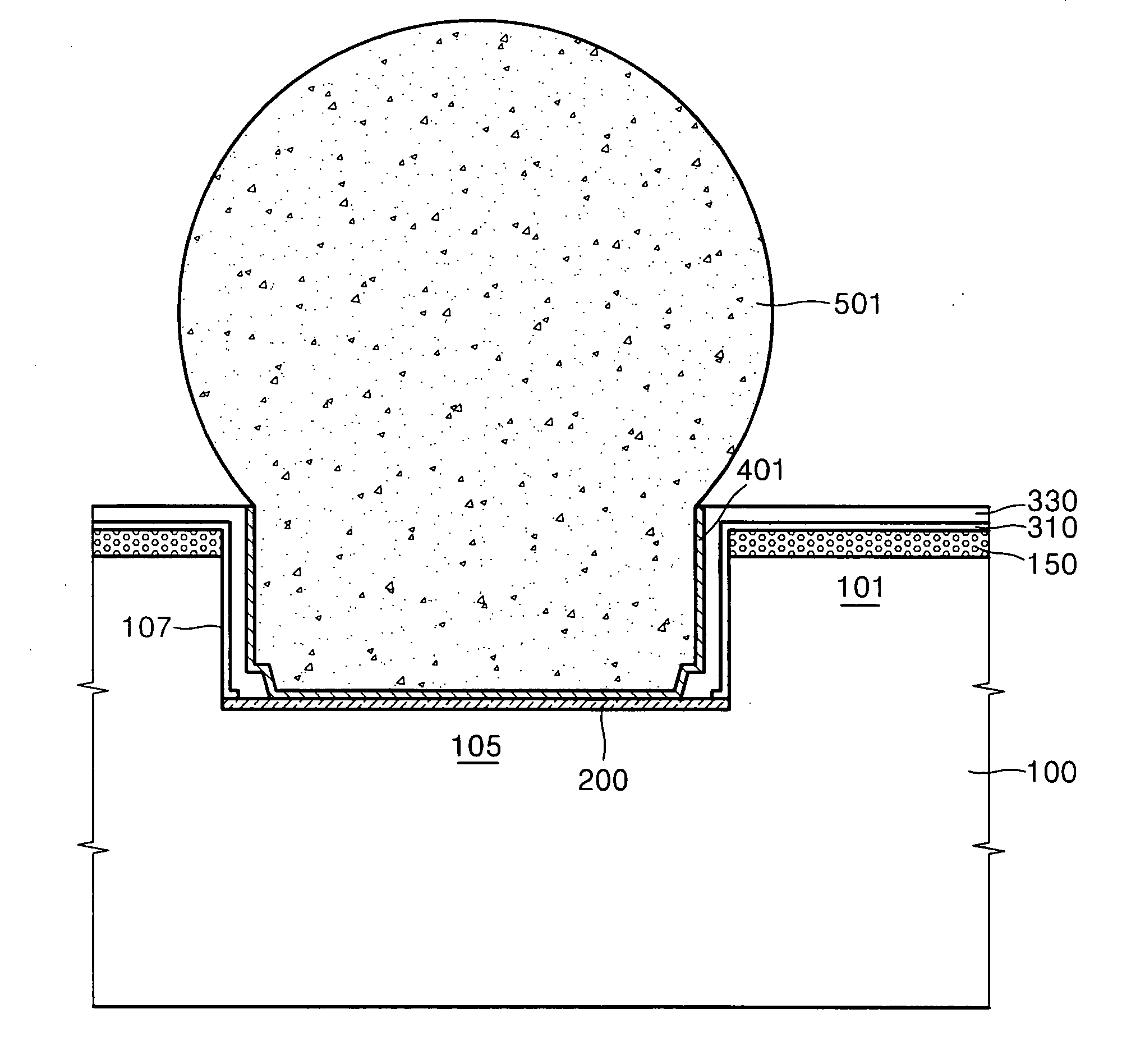
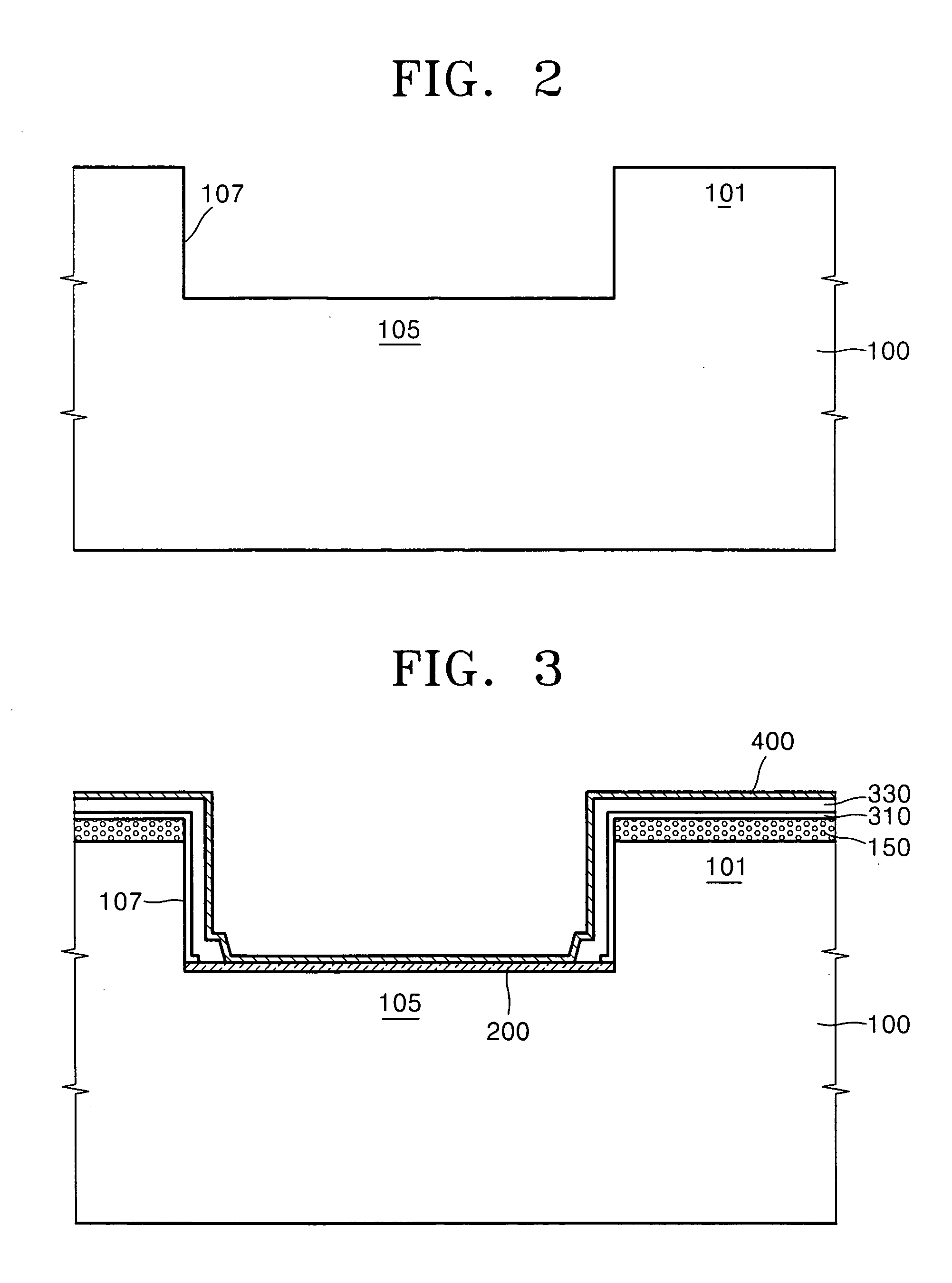
[0040] Referring to FIG. 2, a groove 107 in which a lower end portion of a bump will be partially buried is formed in a wafer or a semiconductor substrate, e.g., a silicon semiconductor substrate 100. That is, the groove 107 is formed in a bump pad region 105 of the semiconductor substrate 100 where the bump will be formed or bonded. The groove 107 may have a deep trench geometry, and may be placed where the bump pads are formed when considering the structure of the semiconductor device.

[0041] A depth of the groove 107 is determined in consideration of the thickness and the diameter of the resulting desired bump, which is several μm to several tens of μm deep.

[0042] The groove 107 can be formed to be several tens of μm deep when considering the height of the resulting bump in one example, when the thickness or diameter of...

second embodiment

[0056]FIGS. 7 through 9 are sectional views illustrating a bump structure of a semiconductor device according to the present invention.

[0057] Referring to FIG. 7, a mask pattern 115 as a sacrificial layer for forming the groove is formed on a bump pad region 105 of a semiconductor substrate 100 or Silicon On Insulator (SOI) substrate to which a bump is formed or attached. The mask pattern 115 is formed to cover the bump pad region 105 and to expose a device region 101 where the device will be formed. The mask pattern 115 can optionally be composed of an insulating material such as silicon oxide or silicon nitride. Also, the thickness of the mask pattern 115 is determined by considering the resulting depth of the desired groove to be formed.

[0058] Thereafter, a selective epitaxial growth procedure is performed to the silicon surface of the semiconductor substrate 100 exposed by the mask pattern 115, thereby forming a semiconductor layer 110 on which devices will be formed. Preferabl...


PUM


Abstract

In connection with a bump of a semiconductor device and a manufacturing method thereof, a groove is formed in a bump pad region of a semiconductor substrate. An under bump metal layer is then formed in the groove, and a lower end portion of the bump fills the groove on the under bump metal layer.

Description

CROSS-REFERENCE TO RELATED PATENT APPLICATION [0001] This application claims the benefit of Korean Patent Application No. 10-2005-0007984, filed on Jan. 28, 2005, in the Korean Intellectual Property Office, the disclosure of which is incorporated herein in its entirety by reference. BACKGROUND OF THE INVENTION [0002] 1. Field of the Invention [0003] The present invention relates to a semiconductor device, and more particularly to a bump for an electrical connection in a semiconductor device package and a method of manufacturing the same. [0004] 2. Description of the Related Art [0005] Various techniques for packaging integrated circuit (IC) chips or semiconductor device chips integrated with ICs have been suggested in the semiconductor manufacturing arts. The increase of the integration density in semiconductor devices has led to the popularity of bump pad technology, particularly having a small pitch. Minimized and / or portable electronic appliances employing semiconductor device pa...

Claims


Application Information

Patent Timeline
Patent Type & Authority Applications(United States)
IPC IPC(8): H01L23/48H01L21/44
CPCH01L24/03H01L24/05H01L2924/0002H01L2224/05571H01L2924/00014H01L2924/01033H01L2924/19041H01L24/11H01L24/12H01L2224/03912H01L2224/0401H01L2224/05599H01L2224/13022H01L2224/13099H01L2924/01013H01L2924/01014H01L2924/01029H01L2924/01078H01L2924/01079H01L2924/014H01L2924/05042H01L2924/14H01L2924/00012H01L2224/05552H01L2224/0361H01L2224/11462H01L2224/1147H01L2224/11849
Inventor KO, YOUNG-PIL
Owner SAMSUNG ELECTRONICS CO LTD
Why Eureka
Try Eureka