

Plasma display panel and method of manufacturing the same
- Summary
- Abstract
- Description
- Claims
- Application Information
AI Technical Summary
Benefits of technology
Problems solved by technology
Method used
Image

Examples
first embodiment
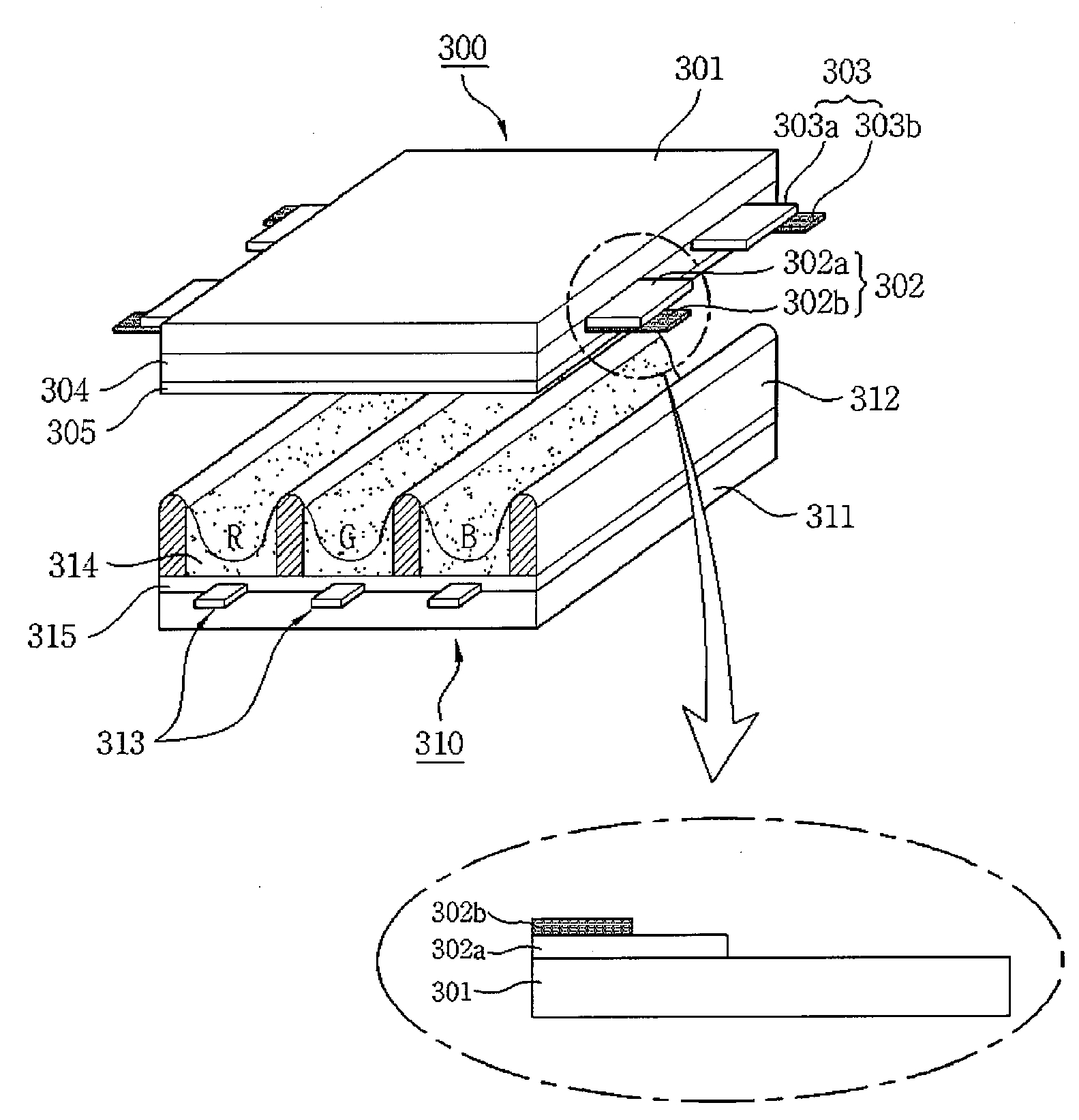
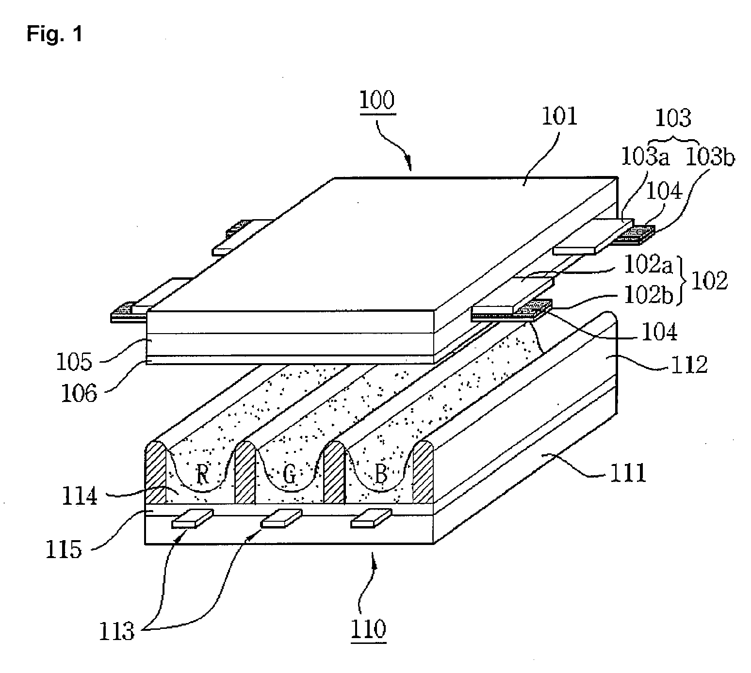
[0043]FIG. 3 illustrates the structure of the PDP according to the first embodiment of the present invention.
[0044] Referring to FIG. 3, in the PDP according to the first embodiment of the present invention, a front panel 300 obtained by arranging a plurality of pairs of sustain electrodes formed of scan electrodes 302 and sustain electrodes 303 that make pairs and a rear panel 310 obtained by arranging a plurality of address electrodes 313 to intersect the plurality of pairs of sustain electrodes are combined with each other to run parallel to each other by a uniform distance.
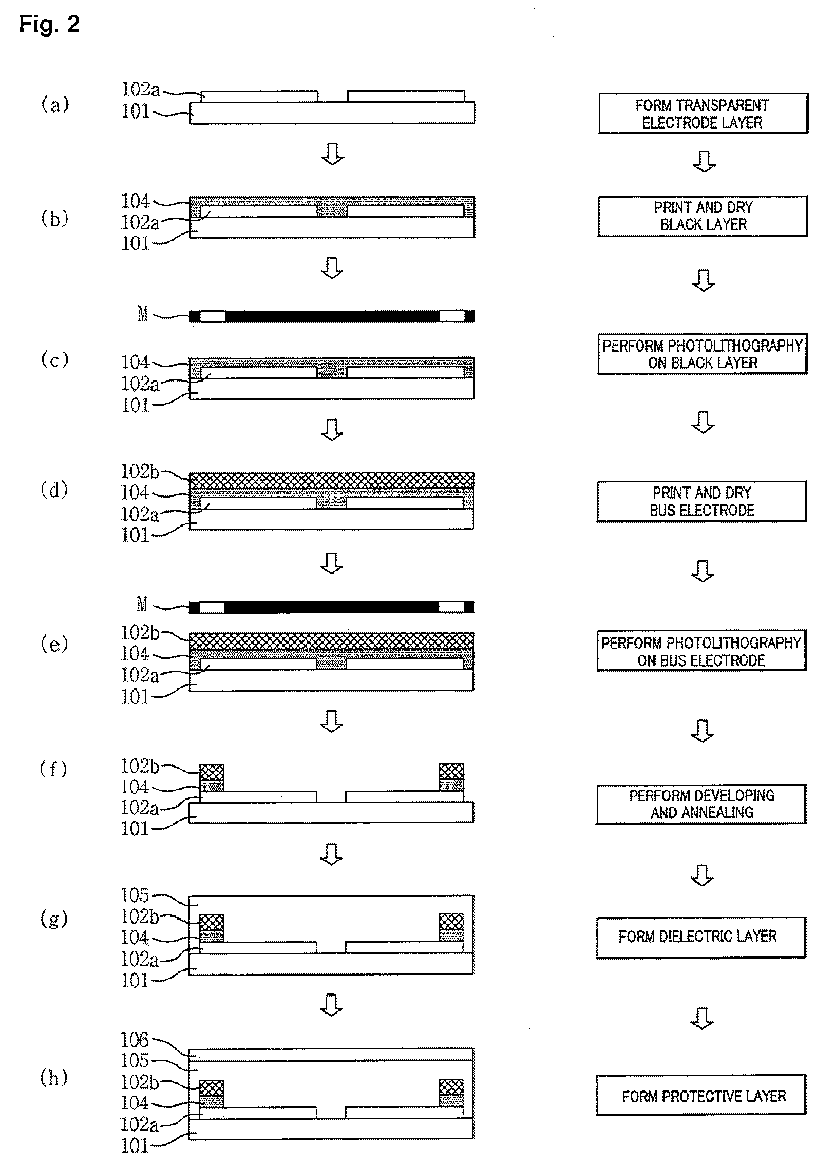
[0045] In the front panel 300, the scan electrode 302 and the sustain electrode 303 for discharging each other in one discharge cell to sustain emission of the cell are formed on a front glass 301. The scan electrode 302 and the sustain electrode 303 comprise transparent electrodes 302a and 303a made of a transparent material and bus electrodes 302b and 303b comprising a black material.
[0046] The transparen...
second embodiment
[0072]FIG. 6 illustrates the structure of the PDP according to the second embodiment of the present invention.
[0073] Referring to FIG. 6, the structure of the PDP according to the second embodiment of the present invention is almost the same as the structure of the PDP according to the first embodiment of the present invention. Therefore, description of the same structure as the structure of the PDP according to the first embodiment of the present invention will be omitted. In the PDP according to the second embodiment of the present invention, a scan electrode 402 and a sustain electrode 403 do not comprise transparent electrodes but comprise only bus electrodes 402b and 403b.
[0074] The PDP according to the second embodiment of the present invention having the above structure has the effects of the PDP according to the first embodiment of the present invention. Furthermore, the transparent electrodes are omitted so that it is possible to reduce the manufacturing cost.
[0075]FIG. ...
PUM
 Abstract
Description
Claims
Application Information