Current sensor
a current sensor and current technology, applied in the field of current sensors, can solve the problems of difficult detection of weak currents and unfavorable miniaturization, and achieve the effects of reducing the overall dimension, reducing the influence of heat generated, and efficient detection of the first magnetic field
- Summary
- Abstract
- Description
- Claims
- Application Information
AI Technical Summary
Benefits of technology
Problems solved by technology
Method used
Image
Examples
first embodiment
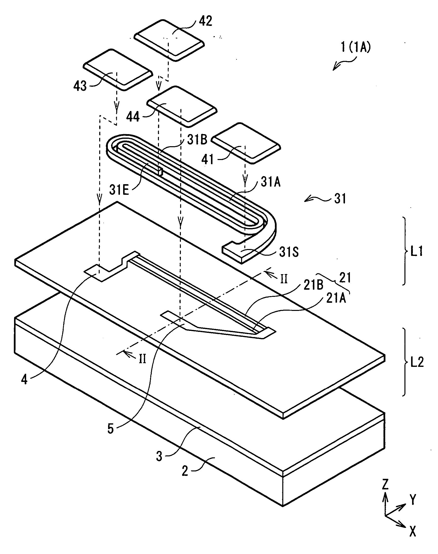
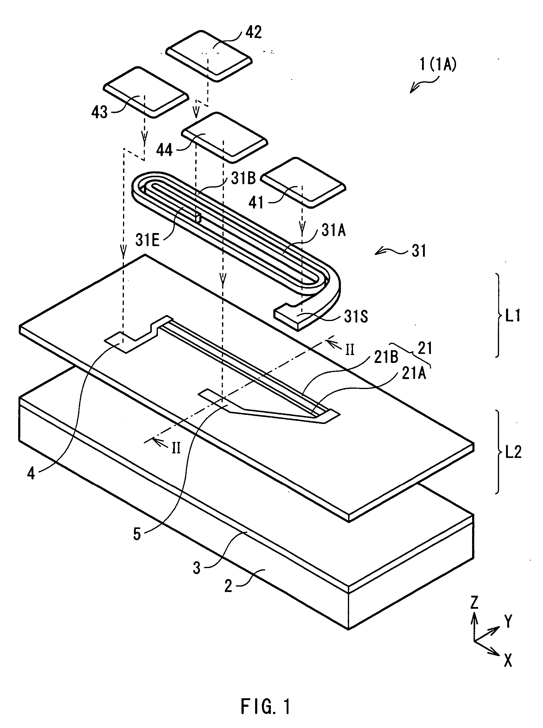
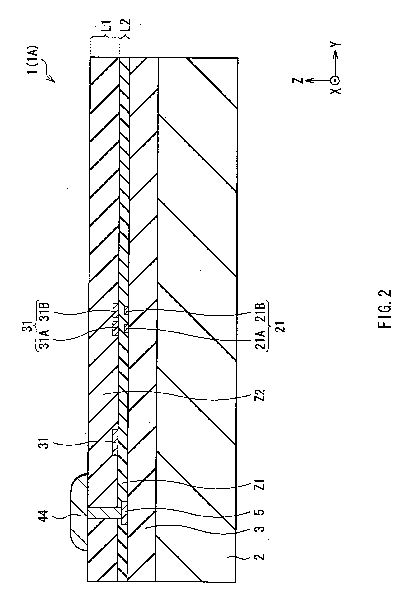
[0045] Reference to FIGS. 1 and 2, the configuration of a current sensor as a first embodiment of the invention will be described. FIG. 1 is a schematic view illustrating a perspective configuration of a current sensor 1 according to the embodiment. FIG. 2 shows a cross-sectional configuration taken along line II-II in the current sensor 1 of FIG. 1, looking in the direction of the appended arrows (−X-axis direction). The current sensor 1 is mounted on, for example, communication equipment, and used to accurately detect and measure a current of a control signal. In particular, current in the range of 10 mA to 50 mA is detected here. To distinguish the current sensor of the first embodiment from that in embodiments to be described later, the current sensor in the first embodiment is hereinafter referred to as a current sensor 1A.
[0046] The current sensor 1A includes a first thin film coil 31 as a first conductor disposed in a first layer L1, and a first magnetoresistive element 21 d...
modification 1
[0070] Although the first embodiment describes the case of measuring a current Im which is in the range of 10 mA to 50 mA, it is possible to configure a current sensor so as to measure a weaker current Im, for example, in the range of 3 mA to 50 mA. In this case, the distance D1 as shown in the sectional view of FIG. 3 is in the range of 0.2 μm to 0.4 μm (Conditional expression 3). This is because the turn portion 31A and the element pattern 21A need to be closer in order to detect a magnetic field Hm1 formed by a weaker current Im as low as less than or equal to 10 mA. On the other hand, setting at more than or equal to 0.2 μm makes it possible to withstand an application of a surge voltage of 700 V. This is practically favorable.
[0071] The cross-sectional area S1 (=MX*MY1) in the turn portion 31A is in the range of 0.4 μm2 to 2.5 μm2 (Conditional expression 4). When the cross-sectional area S1 is less than 0.4 μm2, a current Im flowing through the turn portion 31A causes an exces...
second embodiment
[0073] Reference to FIGS. 11 to 13, a current sensor 1B as a second embodiment of the invention will be described below.
[0074]FIG. 11 is a perspective view showing a perspective configuration of the current sensor 1B. FIG. 12 shows a cross-sectional configuration in the direction indicated by the arrows (−X direction) along the line XII-XII of the current sensor 1B shown in FIG. 11. The current sensor 1B can be obtained by adding a second thin film coil 32 (hereinafter referred to simply as a thin film coil 32) as a second conductor, to the current sensor 1A of the above embodiment.
[0075] Specifically, with respect to a second layer L2, a third layer L3 is provided on the side opposite to a first layer L1 in the current sensor 1B, and the thin film coil 32 is formed so as to be buried in an insulating film Z3 in the third layer L3. In other words, as shown in FIG. 12, the current sensor 1B has such a structure that the third layer L3 including the thin film coil 32, the second lay...
PUM
 Abstract
Description
Claims
Application Information


