Vertical cavity surface-emitting semiconductor laser device, optical transmission module, optical transmission device, and optical switching method

a semiconductor laser and optical transmission module technology, applied in semiconductor lasers, laser details, electrical equipment, etc., can solve the problems of high cost of external modulator systems, large number of parts needed, and difficulty in operating existing semiconductor lasers at modulation frequencies exceeding 10 ghz by direct modulation methods, etc., to achieve reliable suppression of the change of carrier density in the active layer and higher speed

Inactive Publication Date: 2006-08-03
RICOH KK
View PDF5 Cites 22 Cited by
  • Summary
  • Abstract
  • Description
  • Claims
  • Application Information

AI Technical Summary

Benefits of technology

[0025] According to the vertical cavity surface-emitting semiconductor laser device, the optical transmission module, the optical transmission device, and the optical switching method of the present invention, it is p...

Problems solved by technology

However, it is difficult to operate the existing semiconductor laser at a modulation frequency exceeding 10 GHz by using the direct modulation method.
However, in the case of the external modulator system, the module size is large, the number of parts needed is also large, and there is a problem that the external modulator system is expensive.
Therefore, even if the optical transmission technology employing the external modulator can be used for an expensive system such as the trunk system, it is unsuitable for the systems used by the ordinary users, such as LAN systems or ho...

Method used


Image

  • Vertical cavity surface-emitting semiconductor laser device, optical transmission module, optical transmission device, and optical switching method
  • Vertical cavity surface-emitting semiconductor laser device, optical transmission module, optical transmission device, and optical switching method
  • Vertical cavity surface-emitting semiconductor laser device, optical transmission module, optical transmission device, and optical switching method

Examples


Embodiment Construction

[0051] A description will now be given of an embodiment of the invention with reference to the accompanying drawings.

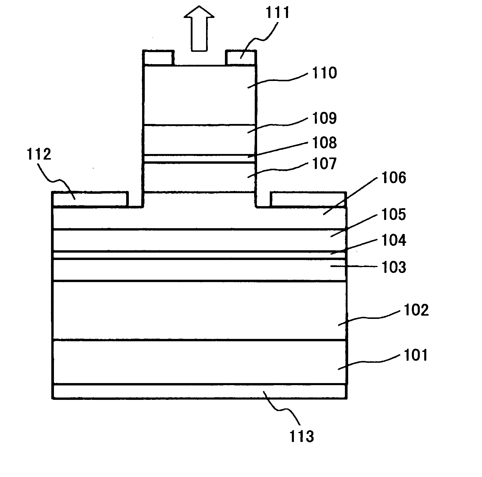
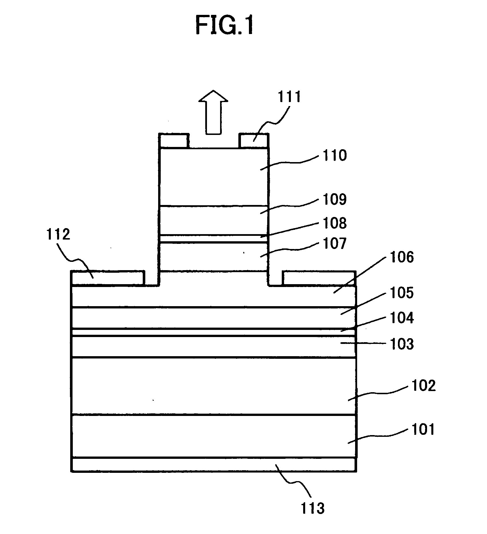
[0052]FIG. 1 shows the composition of a vertical cavity surface-emitting semiconductor laser device (VCSEL) in an embodiment of the invention.

[0053] Referring to FIG. 1, a lower distribution Bragg reflector (DBR) 102 of a 1st conductivity type, a 1st spacer layer 103, an active layer 104, a 2nd spacer layer 105, a DBR 106 of a 2nd conductivity type, a 3rd spacer layer 107, an optical absorption layer 108, a 4th spacer layer 109, and an upper DBR 110 of the 1st conductivity type are deposited sequentially on a semiconductor monocrystal substrate 101 of the 1st conductivity type.

[0054] The DBR is formed such that a high refractive index layer and a low refractive index layer are laminated alternately by ¼ of the optical length of an oscillation wavelength. The region between the lower DBR 102 of the 1st conductivity type and the DBR 106 of the 2nd conductivity type h...


PUM


Abstract

In a vertical cavity surface-emitting semiconductor laser device, first and second resonance wavelengths which are different are provided while a first resonator and a second resonator are coupled optically, and a gain of an active layer at the first resonance wavelength on the side of short wavelength is higher than that at the second resonance wavelength on the side of long wavelength. An absorption coefficient of an optical absorption layer when no electric field is applied is small for the first and second resonance wavelengths, and when an electric field is applied, an absorption coefficient of the optical absorption layer for the first resonance wavelength on the side of short wavelength is larger than that for the second resonance wavelength on the side of long wavelength.

Description

BACKGROUND OF THE INVENTION [0001] 1. Field of the Invention [0002] The present invention relates to a vertical cavity surface-emitting semiconductor laser device, an optical transmission module, an optical transmission device, and an optical switching method. [0003] 2. Description of the Related Art [0004] In recent years, the optical transmission technology has been developed to not only the trunk-system transmission network but also LAN, the access system and the home network. For example, in the Ethernet, the data-transmission capacity of 10 Gbps has been developed. In the future, a further increase in the data-transmission capacity is demanded, and an optical transmission system with the transmission capacity of over 10 Gbps is expected. [0005] In the light source for optical transmission the data-transmission capacity of which is 10 Gbps or less, a direct modulation method which modulates the output light intensity by modulating the introducing current of a semiconductor laser...

Claims


Application Information

Patent Timeline
IPC IPC(8): H01S5/00
CPCB82Y20/00H01S5/0425H01S5/06226H01S5/1021H01S5/18302H01S5/18308H01S5/18311H01S5/1833H01S5/18358H01S5/2063H01S5/34306H01S5/3432H01S5/04257H01S5/18341
Inventor TAKAHASHI, TAKASHI
Owner RICOH KK
Why Eureka
Try Eureka