Multi-layer registration and dimensional test mark for scatterometrical measurement

a scatterometric and multi-layer technology, applied in the field of apparatus and method for evaluating semiconductors, can solve problems such as short circuiting, interruption of conduction pathways, and variation in the performance of finished semiconductors

Inactive Publication Date: 2006-08-03
BELL SEMICON LLC
View PDF11 Cites 9 Cited by
  • Summary
  • Abstract
  • Description
  • Claims
  • Application Information

AI Technical Summary

Benefits of technology

[0012] The present invention has been developed in response to the present state of the art, and in particular, in response to the problems and needs in the art that have not yet been fully solved by currently availab...

Problems solved by technology

Each step in the process may have random variation, which in turn may cause variation in the performance of the finished semiconductor.
Misalignment of the mask may cause problems, such as short circuiting, interrupted conduction pathways, or malformed transistors.
Variation in the CD may result in conductive paths that are too wide, bridging into neighboring conduct...

Method used


Image

  • Multi-layer registration and dimensional test mark for scatterometrical measurement
  • Multi-layer registration and dimensional test mark for scatterometrical measurement
  • Multi-layer registration and dimensional test mark for scatterometrical measurement

Examples


Embodiment Construction

[0030] Reference throughout this specification to “one embodiment,”“an embodiment,” or similar language means that a particular feature, structure, or characteristic described in connection with the embodiment is included in at least one embodiment of the present invention. Thus, appearances of the phrases “in one embodiment,”“in an embodiment,” and similar language throughout this specification may, but do not necessarily, all refer to the same embodiment.

[0031] Furthermore, the described features, advantages, and characteristics of the invention may be combined in any suitable manner in one or more embodiments. One skilled in the relevant art will recognize that the invention can be practiced without one or more of the specific features or advantages of a particular embodiment. In other instances, additional features and advantages may be recognized in certain embodiments that may not be present in all embodiments of the invention.

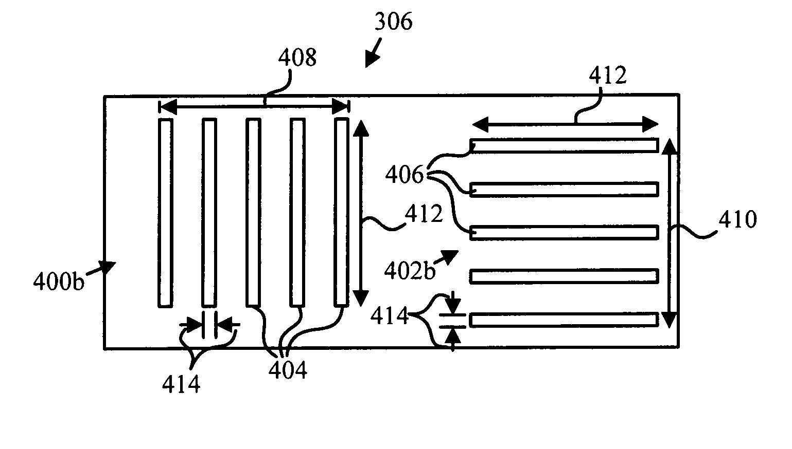
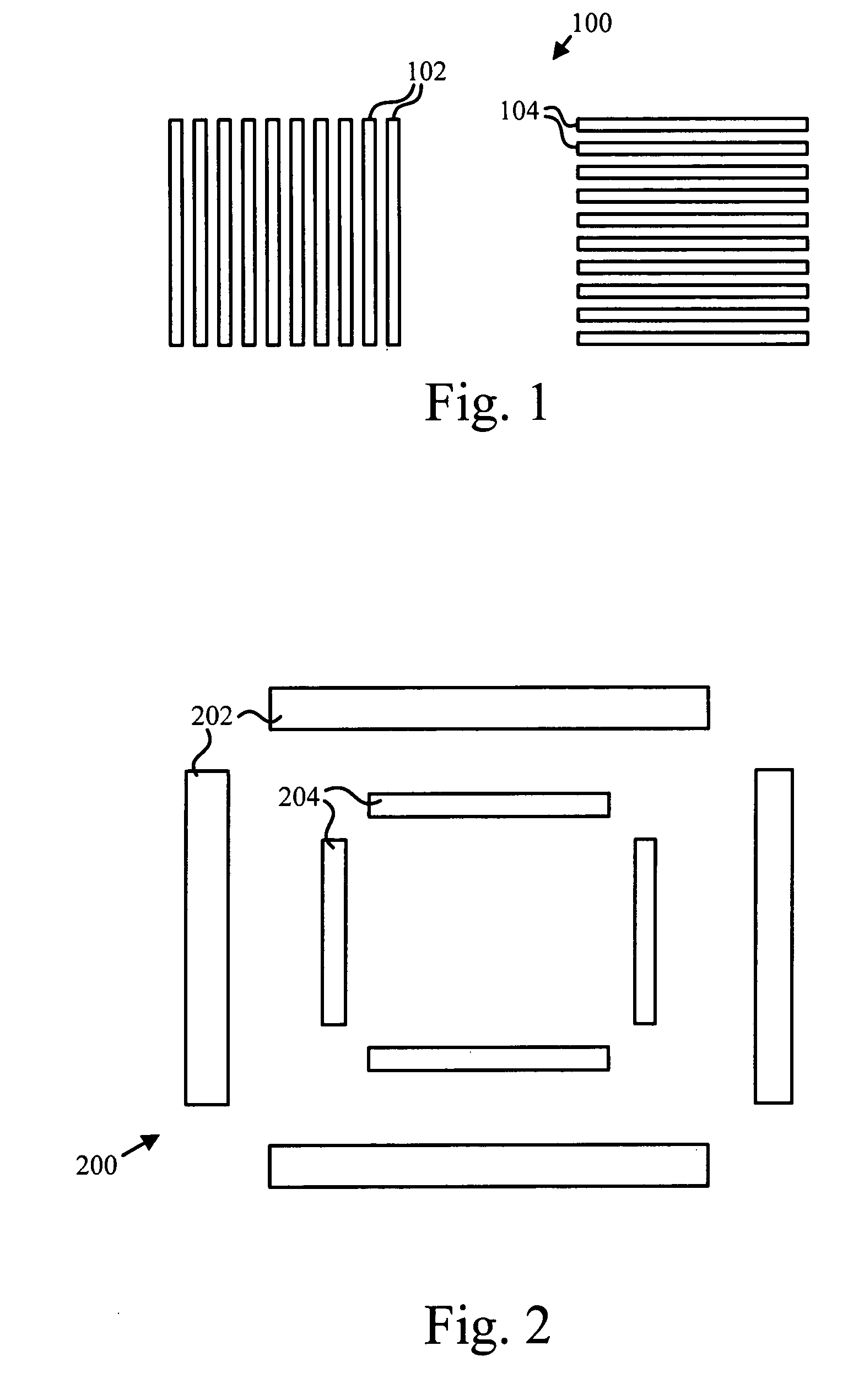
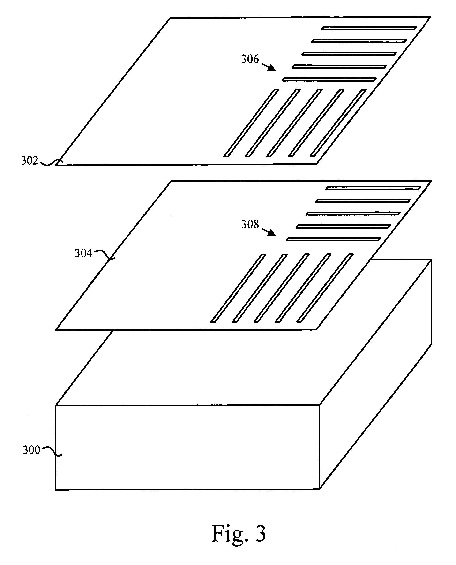
[0032] Referring to FIG. 3, a semiconductor 300,...


PUM


Abstract

A layered test pattern for measuring registration and critical dimension (CD) for multi-layer semiconductor integrated circuits is disclosed. A first layer includes a first pattern having vertical and horizontal portions. A second layer is formed over the first layer and includes a second pattern having vertical and horizontal portions having nominal vertical and horizontal phase shifts with respect to the vertical and horizontal portions, respectively, of the first pattern. The vertical and horizontal portions include periodically repeating vertical lines and horizontal lines, respectively. The nominal phase shifts may be half of the period of the vertical and horizontal lines. A scatterometry tool measures the width of the lines and the phase shift of the first pattern relative to the second pattern. The width of the lines corresponds to CD, whereas the difference between the measured phase shift and the nominal phase shift indicates variation in registration.

Description

BACKGROUND OF THE INVENTION [0001] 1. Field of the Invention [0002] The invention relates generally to apparatus and method for evaluating semiconductors, and more particularly to apparatus and method for measuring the registration and critical dimension (CD) of deposited layers. [0003] 2. Description of the Related Art [0004] The need for faster and faster semiconductor integrated circuits (IC) has resulted in a decrease in the size of electronic elements formed on semiconductors, such as transistors and conductive paths. As a result, process variations during manufacture of semiconductors must be more accurately measured and more tightly controlled. [0005] A typical integrated circuit is formed on a substrate wafer made of silicon or another semiconductor, such as gallium arsenide (GaAs) and indium phosphide (InP). The substrate then undergoes various processes such as layering, oxidation, etching, and doping in order to form transistors and conductive paths thereon. Layering typi...

Claims


Application Information

Patent Timeline
IPC IPC(8): H01L21/00
CPCG03F7/70625G03F7/70633G03F7/70683H01L23/544H01L2223/54466H01L2924/0002H01L2924/00
Inventor DO, PHONG THANHROLOFSON, KIRKSTURTEVANT, DAVID
Owner BELL SEMICON LLC
Why Eureka
Try Eureka