Screen printable electrode for light emitting polymer device

a polymer device and screen printing technology, applied in the field of electroluminescent device fabrication, can solve the problems of easy oxidation of low work function metals upon exposure to air, shorting and device failure, and increasing the complexity and cost of fabricating lep devices, and achieve the effect of inexpensive fabrication of electroluminescent devices

Inactive Publication Date: 2006-08-03
SUMITOMO CHEM CO LTD
View PDF52 Cites 18 Cited by
  • Summary
  • Abstract
  • Description
  • Claims
  • Application Information

AI Technical Summary

Benefits of technology

[0017] The present invention discloses the important process step of screen printing the top electrode in LEP device construction under normal atmospheric conditions. This process step

Problems solved by technology

One layer, the top electrode, has not previously been screen printable (i.e. via liquid processes under atmospheric conditions) which greatly increases the complexity and cost of fabricating LEP devices.
Screen printing an electrode on top of such soft thin films invariably leads to shorting and device failure.
However, low work-function metals readily oxidized upon exposure to air.
Heretofore, top cathodes for forward-build LEP devices have not been screen printable.
Their lower conductivity restricts their applicability in LEP devices, which have a relatively high electrical current requirements.
The low conductivity of the organic pastes can cause a significant voltage drop between the power supply and the LEP light emitting

Method used


Image

  • Screen printable electrode for light emitting polymer device
  • Screen printable electrode for light emitting polymer device
  • Screen printable electrode for light emitting polymer device

Examples


Embodiment Construction

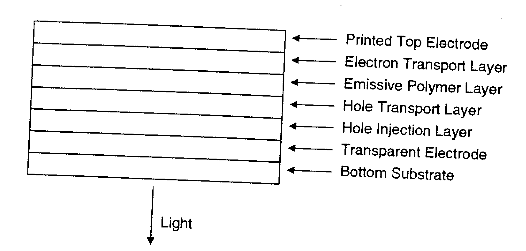
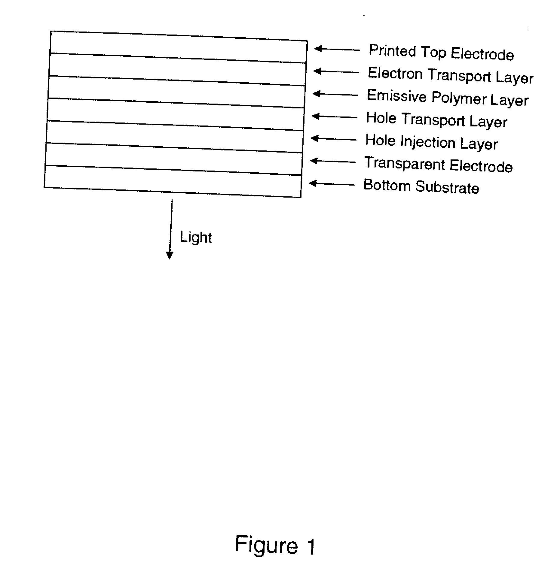
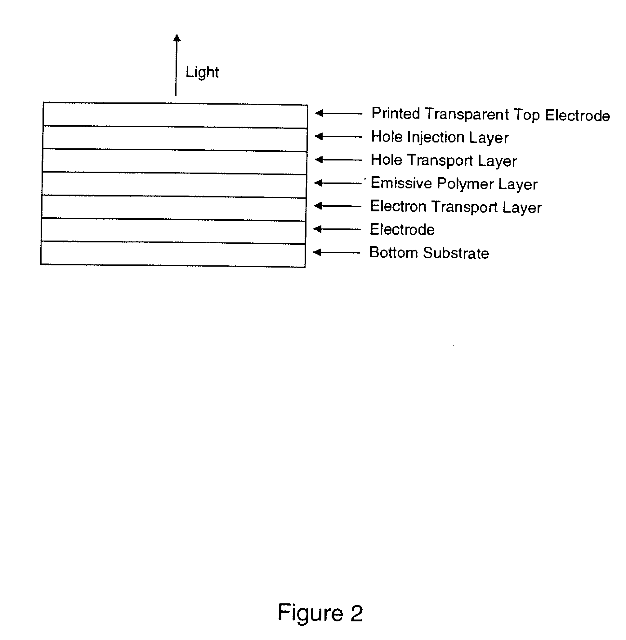
[0023] The present invention will now be described in detail with reference to the drawings, which are provided as illustrative examples of the invention so as to enable those skilled in the art to practice the invention. Notably, the figures and examples below are not meant to limit the scope of the present invention. Moreover, where certain elements of the present invention can be partially or fully implemented using known components, only those portions of such known components that are necessary for an understanding of the present invention will be described, and detailed descriptions of other portions of such known components will be omitted so as not to obscure the invention. Further, the present invention encompasses present and future known equivalents to the known components referred to herein by way of illustration.

[0024] The present invention includes three methods to screen print a top electrode that avoids shorts in LEP devices.

[0025] In one embodiment of the present ...


PUM

PropertyMeasurementUnit
Diameteraaaaaaaaaa
Diameteraaaaaaaaaa
Electrical conductivityaaaaaaaaaa

Abstract

A screen printed light emitting polymer device is fabricated by depositing an electroluminescent polymer layer between a transparent electrode and an air stable screen printed top electrode. This invention describes advantageous methods and materials for printed top electrodes for polymer light emitting devices including composite electrode inks containing conducting particles, ionic, semiconducting and non-conducting components. These improvements can simplify device processing and costs as well as improve device performance in terms of voltage, prevention of shorting, operating lifetime and other metrics.

Description

[0001] This is a division of U.S. patent application. Ser. No. 10 / 327,632 filed Dec. 20, 2002, and claims priority to U.S. Provisional Patent Application No. 60 / 342,579 filed Dec. 20, 2001 entitled “Screen Printable Electrode for Light Emitting Polymer Device”, the contents of which are incorporated herein by reference.FIELD OF THE INVENTION [0002] The present invention relates to electroluminescent devices, and more particularly to the fabrication of electroluminescent devices. BACKGROUND OF THE INVENTION [0003] Light-emitting polymer (LEP) devices have been under development for back-lighting in liquid crystal displays and instrument panels, and to replace vacuum fluorescent and liquid crystal displays. There are several patents (see references 1-3) that teach how different LEP device layers enable the efficient production of electroluminescent light. For instance, U.S. Pat. No. 6,284,435 to Cao discloses electrically active polymer compositions and their use in efficient, low ope...

Claims


Application Information

Patent Timeline
IPC IPC(8): H01L21/00H01L27/32H05B33/26H01L51/00H01L51/30H01L51/40H01L51/50H01L51/52H05B33/10
CPCH01L27/32H01L51/0022H01L51/0023H01L51/0037H01L51/0038H01L51/5048H01L51/5203H01L51/5206H01L51/5221H01L2251/5315H10K71/611H10K71/621H10K85/114H10K85/1135H10K50/15H10K50/16H10K50/81H10K50/82H10K2102/331H10K2102/3026H10K50/805H10K59/00
Inventor CARTER, SUSAN A.VICTOR, JOHN G.
Owner SUMITOMO CHEM CO LTD
Why Eureka
Try Eureka