

Method of forming a two-layer gate dielectric
- Summary
- Abstract
- Description
- Claims
- Application Information
AI Technical Summary
Benefits of technology
Problems solved by technology
Method used
Image

Examples
Embodiment Construction
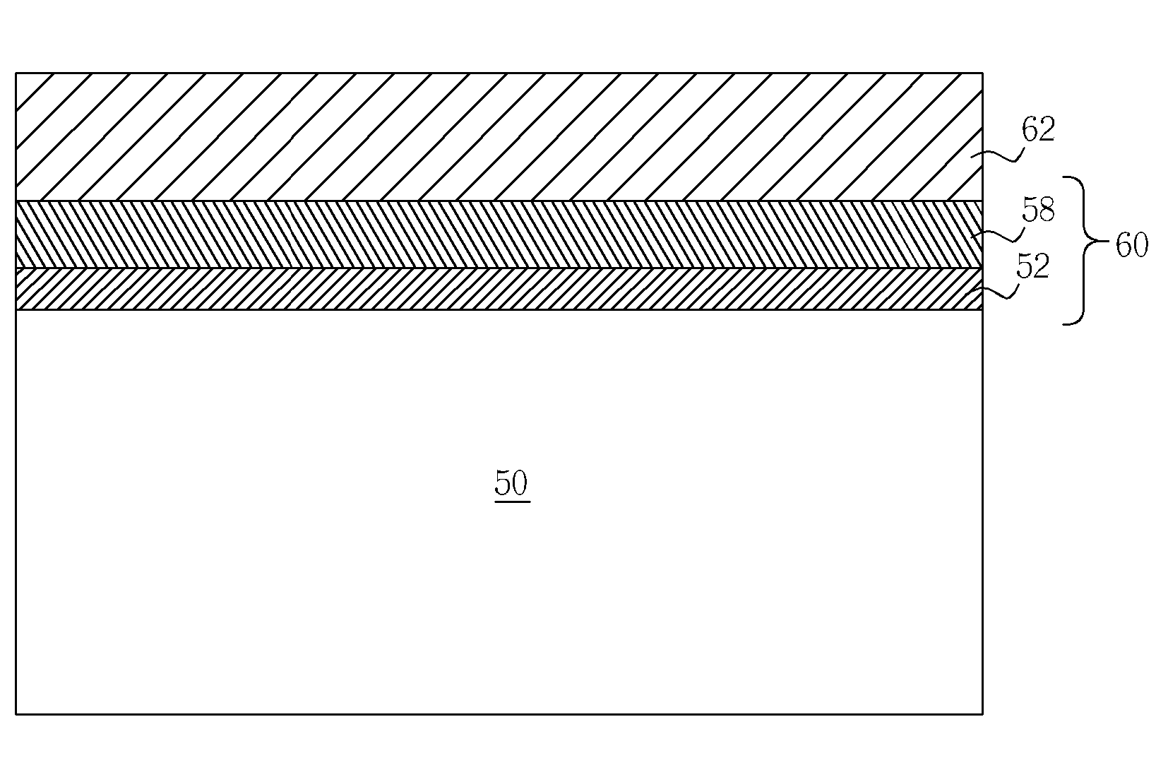
[0013] Please refer to FIG. 5 through FIG. 10. FIG. 5 through FIG. 10 are schematic diagrams illustrating a method of forming a two-layer gate dielectric according to a preferred embodiment of the present invention. As shown in FIG. 5, a substrate 50, such as a silicon substrate, is provided, and a silicon dioxide thin film 52 is formed on the substrate 50. In this embodiment, the silicon dioxide thin film 52 has a thickness of between 5 to 80 angstroms, and is formed using a chemical vapor deposition process at a temperature under 400° C. to ensure a good interface between the substrate 50 and the silicon dioxide thin film 52. However, the formation of the silicon dioxide thin film 52 is not limited by this, and can be implemented by other processes, e.g. a thermal oxidation process.
[0014] As shown in FIG. 6, an amorphous silicon thin film 54 is formed on the silicon dioxide thin film 52. In this embodiment, the amorphous silicon thin film 54 has a thickness of less than 10 angstr...
PUM
 Abstract
Description
Claims
Application Information