Semiconductor device including FinFET having metal gate electrode and fabricating method thereof

a technology of semiconductor devices and finfets, which is applied in the direction of semiconductor devices, brassieres, electrical equipment, etc., can solve the problems of difficult to reduce the size of conventional mosfets, difficult to inhibit the short channel effect, and short gap between source and drain of semiconductor devices

Inactive Publication Date: 2006-08-10
SAMSUNG ELECTRONICS CO LTD
View PDF6 Cites 371 Cited by
  • Summary
  • Abstract
  • Description
  • Claims
  • Application Information

AI Technical Summary

Benefits of technology

[0023]FIG. 21 is a graph showing a counter doping effect in a method of fabricating a semiconductor device according to an embodiment of the present invention.

Problems solved by technology

However, in this case, a gap between a source and a drain of the semiconductor device is shortened.
In such a device, it is difficult to reduce the size of the conventional MOSFET.
Also, in a planar device, it is difficult to inhibit the short channel effect from occurring.
However, in conventional FinFETs, a threshold voltage is low due to a thin body effect.
Thus, it is difficult to operate CMOS circuits without degrading the performance of the FinFETs.
However, the work function engineering is difficult to be realized in the operation of CMOS devices.

Method used


Image

  • Semiconductor device including FinFET having metal gate electrode and fabricating method thereof
  • Semiconductor device including FinFET having metal gate electrode and fabricating method thereof
  • Semiconductor device including FinFET having metal gate electrode and fabricating method thereof

Examples


first embodiment

[0024] First Embodiment

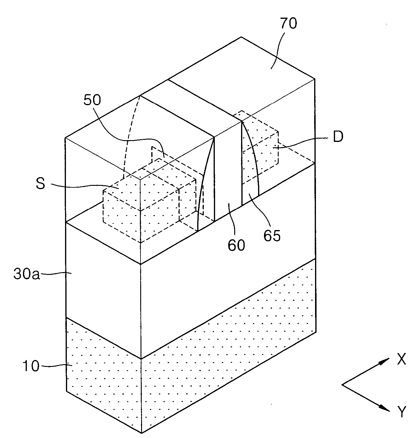
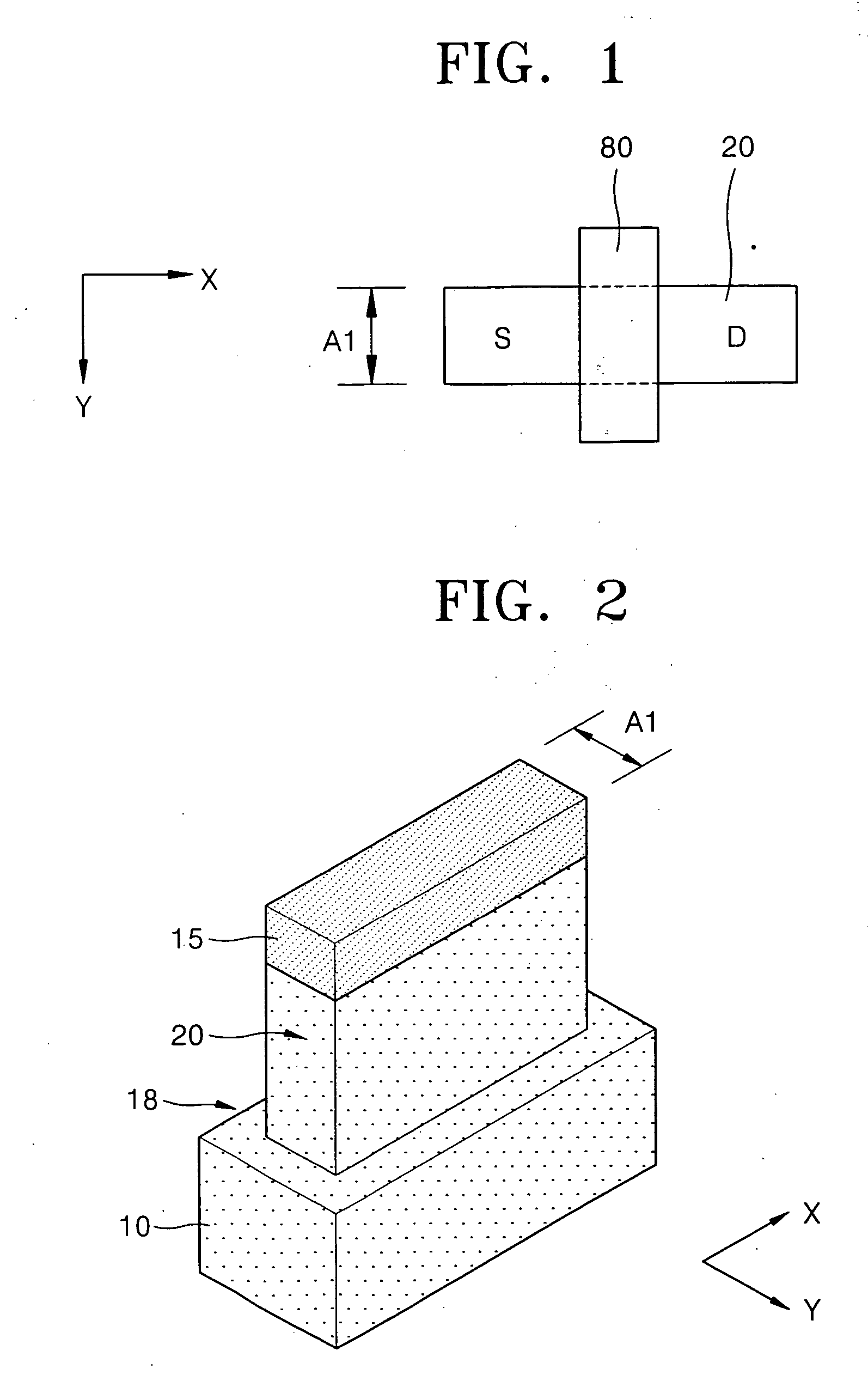
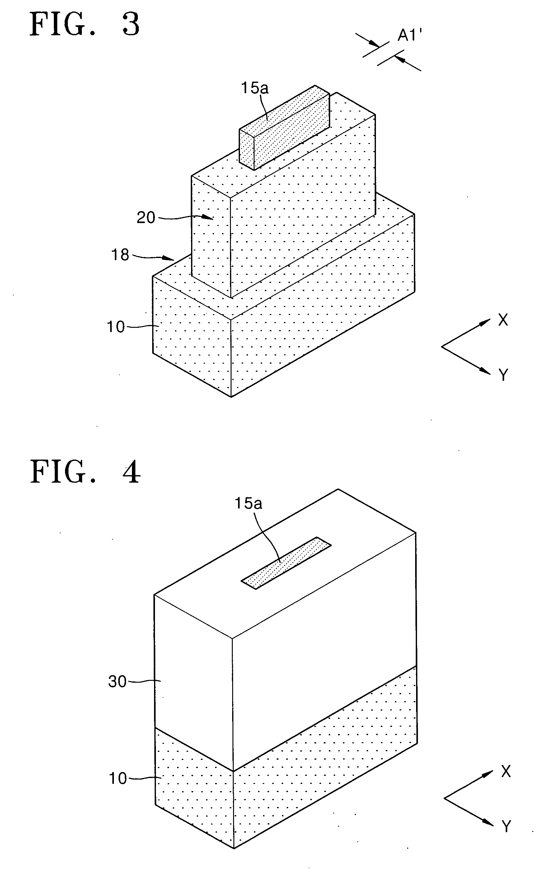
[0025]FIG. 1 is a layout view of a semiconductor device to be fabricated using methods of fabricating a semiconductor device according to first through third embodiments of the present invention. Referring to FIG. 1, an active area 20 is defined to be extended in one direction, for example, in direction X and has a predetermined line width A1 in direction Y orthogonal to the direction X. A metal gate electrode 80 is formed above the active area 20 to be extended in the direction Y. A source S and a drain D are formed in the active area 20 beside both sides of the metal gate electrode 80.

[0026] As shown in FIG. 1, a width of a contact area formed in the source S and the drain D is greater than a width (a length of a cross-section in the direction X) of the metal gate electrode 80. In the present invention, such a layout can be designed so as to solve a limit to securing a source and / or drain contact area, the limit caused by patterning. However, a layout of a ...

second embodiment

[0048] Second Embodiment

[0049]FIG. 16 is a cross-sectional view of a semiconductor device in direction Y according to a second embodiment of the present invention. The same reference numerals as those in FIGS. 2 through 15 denote like elements, and thus description of theses elements will not be repeated.

[0050] The present embodiment is a modified example of the first embodiment.

[0051] The steps described with reference to FIGS. 2 through 6 are performed as in the first embodiment. When the step described with reference to FIG. 7 is performed, the semiconductor substrate 10 below the opening 45 is etched to a deeper depth than in the first embodiment to define a portion to be used as the fin channel. The blocking layer 40 and the gap fill oxide layer 30 are recessed as described with reference to FIG. 8. However, the gap fill oxide layer 30 is recessed to a shallower depth than the depth of the channel. The steps described with reference to FIGS. 9 through 15 are performed as in t...

third embodiment

[0053] Third Embodiment

[0054]FIG. 17 is a perspective view illustrating a method of fabricating a semiconductor device according to a third embodiment of the present invention. The same reference numerals as those in FIGS. 2 through 7 denote like elements, and thus description of those elements will not be repeated.

[0055] The steps described with reference to FIGS. 2 through 6 are performed as in the first embodiment. The channel area definition pattern 15b exposed in the planarization step described with reference to FIG. 6 is selectively removed with respect to the blocking layer 40, the gap fill oxide layer 30, and the semiconductor substrate 10 using wet or dry etching. The channel area definition pattern 15b formed of the silicon nitride layer may be wet etched using a phosphoric acid strip. Thus, the opening 45 is formed in the position of the channel area definition pattern 15b, and the portion of the surface of the substrate 10 below the opening 45, i.e., the portion of the...


PUM


Abstract

Provided are a semiconductor device including a FinFET having a metal gate electrode and a fabricating method thereof. The semiconductor device includes: an active area formed in a semiconductor substrate and protruding from a surface of the semiconductor substrate; a fin including first and second protrusions formed of a surface of the active area and parallel with each other based on a central trench formed in the active area and using upper surfaces and sides of the first and second protrusions as a channel area; a gate insulating layer formed on the active area including the fin; a metal gate electrode formed on the gate insulating layer; a gate spacer formed on a sidewall of the metal gate electrode; and a source and a drain formed in the active area beside both sides of the metal gate electrode. Here, the metal gate electrode comprises a barrier layer contacting the gate spacer and the gate insulating layer and a metal layer formed on the barrier layer.

Description

CROSS-REFERENCE TO RELATED PATENT APPLICATION [0001] This application claims the benefit of Korean Patent Application No. 10-2005-0011018, filed on Feb. 5, 2005, in the Korean Intellectual Property Office, the disclosure of which is incorporated herein in its entirety by reference. BACKGROUND OF THE INVENTION [0002] 1. Field of the Invention [0003] The present invention relates to a semiconductor device and a fabricating method thereof, and more particularly, to a semiconductor device including a Fin Field Effect Transistor (FinFET) and a fabricating method thereof. [0004] 2. Description of the Related Art [0005] The integration density of semiconductor devices has been continuously increased to improve the performance of the semiconductor devices and reduce fabricating cost for the semiconductor devices. A technique for reducing feature sizes of the semiconductor devices is required to increase the density of the semiconductor devices. [0006] A Metal-Oxide-Semiconductor Field Effec...

Claims


Application Information

Patent Timeline
Patent Type & Authority Applications(United States)
IPC IPC(8): H01L29/76
CPCH01L29/4908H01L29/66545H01L29/66795H01L29/785A41C3/065A41C3/0028A41C3/128A41C3/0007
Inventor KIM, SUNG-MINKIM, DONG-WONKIM, MIN-SANGYUN, EUN-JUNG
Owner SAMSUNG ELECTRONICS CO LTD
Why Eureka
Try Eureka