Silicon oxynitride gate dielectric formation using multiple annealing steps

a technology of silicon oxynitride and gate dielectric, which is applied in the direction of basic electric elements, electrical apparatus, and semiconductor devices. it can solve the problems of gate leakage current increase, unsatisfactory performance, and decreased durability

Active Publication Date: 2006-08-10
APPLIED MATERIALS INC
View PDF26 Cites 70 Cited by
  • Summary
  • Abstract
  • Description
  • Claims
  • Application Information

AI Technical Summary

Benefits of technology

[0009] The present invention provides a method for forming a thin silicon oxynitride layer with desired channel mobility and drive current. The method according to an embodiment of the present invention includes annealing the silicon oxynitride film with 1 to 100 mTorr oxidizing gas, which can be oxygen, nitrous oxide, or nitric oxide, and annealing the silicon oxynitride film with about 1 slm oxygen. The step of annealing the silicon oxynitride film with 1 to 100 mTorr oxidizing gas is performed at a higher temperature and higher pressure than the step of annealing the silicon oxynitride film with about 1 slm oxygen.

Problems solved by technology

Attempts have been made to reduce the thickness of dielectrics, such as reducing the thickness of silicon dioxide (SiO2) dielectrics to below 20 Å. However, the use of SiO2 dielectrics with thicknesses below 20 Å often results in undesirable performance and decreased durability.
In addition, there is typically an undesirable increase in the gate leakage current, i.e., tunneling current, that in turn increases the amount of power consumed by the gate.
Thin SiO2 gate dielectrics may also be susceptible to negative-channel metal-oxide semiconductor (NMOS) hot carrier degradation and to positive-channel metal-oxide semiconductor (PMOS) negative bias temperature instability (NBTI).

Method used


Image

  • Silicon oxynitride gate dielectric formation using multiple annealing steps
  • Silicon oxynitride gate dielectric formation using multiple annealing steps
  • Silicon oxynitride gate dielectric formation using multiple annealing steps

Examples


Embodiment Construction

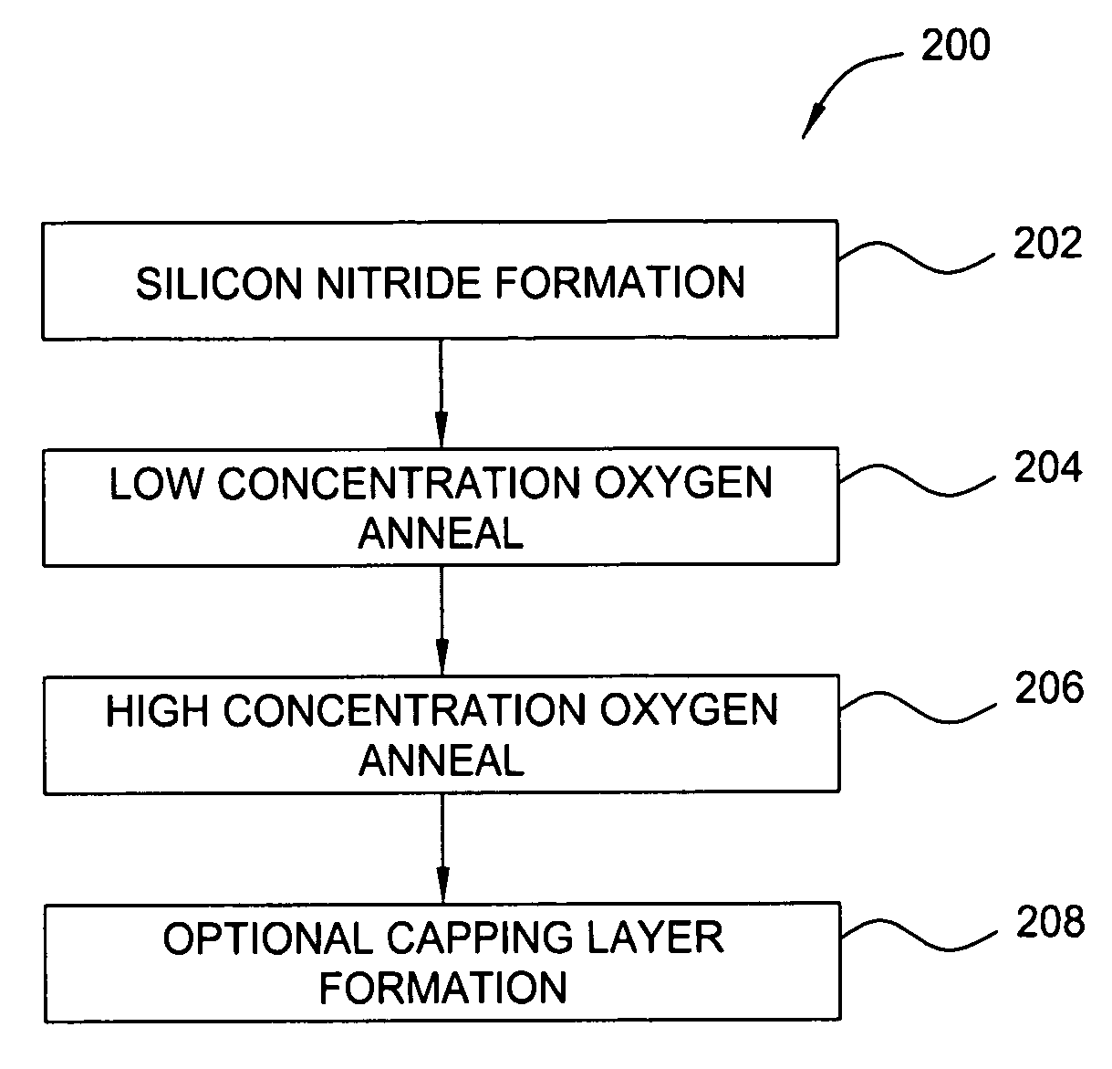
[0014]FIG. 1 is a schematic view of an integrated tool 100 for processing semiconductor substrates according to various embodiments of the present invention. One example of the integrated tool 100 is the GATE STACK CENTURA™ integrated tool from Applied Materials, Inc. of Santa Clara, Calif. The integrated tool 100 includes loadlock chambers 102 and 104, rapid thermal anneal or process (RTP) chambers 106 and 108, a decoupled plasma nitridation (DPN) chamber 110, a deposition chamber 112, and a cool down chamber 114. The integration tool 100 also includes a substrate-handling tool 116 used to transfer a substrate 118 in and out of a particular processing chamber.

[0015] The substrate-handling tool 116 is located in a central transfer chamber in communication with each of the surrounding chambers. The loadlock chambers 102 and 104 house substrates to be processed. The deposition chamber 112 is a chemical or physical vapor deposition chamber that can be used to form a film or layer on a...


PUM

PropertyMeasurementUnit
partial pressureaaaaaaaaaa

Abstract

A method for processing a semiconductor substrate in a chamber includes forming a silicon oxynitride film using a two-step anneal process. The first anneal step includes annealing the silicon oxynitride film in the presence of an oxidizing gas that has a partial pressure of about 1 to about 100 mTorr, and the second anneal step includes annealing the silicon oxynitride film with oxygen gas that has a flow rate of about 1 slm. The first anneal step is performed at a higher chamber temperature and higher chamber pressure than the second anneal step.

Description

CROSS-REFERENCE TO RELATED APPLICATIONS [0001] This application is a continuation-in-part of co-pending U.S. patent application Ser. No. 10 / 794,707, filed Mar. 4, 2004, which claims the benefit of U.S. Provisional Patent Application Ser. No. 60 / 453,057, filed Mar. 7, 2003. Each of the aforementioned related patent applications is herein incorporated by reference.BACKGROUND OF THE INVENTION [0002] 1. Field of the Invention [0003] Embodiments of the present invention generally relate to semiconductor processing including forming a silicon oxynitride film. More specifically, the present invention relates to a method for forming a silicon oxynitride film using plasma nitridation and a two step annealing process. [0004] 2. Description of the Related Art [0005] As device geometries of integrated circuits and transistors have decreased, the gate drive current required by the transistors have increased. It is known that a gate drive current of a transistor increases as its gate capacitance ...

Claims


Application Information

Patent Timeline
Patent Type & Authority Applications(United States)
IPC IPC(8): H01L21/31H01L21/28H01L21/314H01L21/324H01L29/51
CPCH01L21/28185H01L21/28202H01L21/3144H01L21/324H01L21/67207H01L29/518H01L21/0214H01L21/02323H01L21/31H01L21/02329H01L21/02337
Inventor OLSEN, CHRISTOPHER S.
Owner APPLIED MATERIALS INC
Why Eureka
Try Eureka