
Tab tape and method of manufacturing the same

Active Publication Date: 2006-08-17
PANASONIC SEMICON SOLUTIONS CO LTD
View PDF2 Cites 29 Cited by
  • Summary
  • Abstract
  • Description
  • Claims
  • Application Information

AI Technical Summary

Benefits of technology

[0011] In order to solve the problems, an object of a TAB tape and a method of manufacturing the same of the present invention is to reduce a test pad area to miniaturize a semiconductor package such as a tape carrier package without changing the orientation of a semiconductor chip.

Problems solved by technology

Relative to the increasing number of test terminals for simultaneously measuring two chips, the number of channels of a tester is not sufficient and thus equipment has to be modified.

Method used


Image

  • Tab tape and method of manufacturing the same
  • Tab tape and method of manufacturing the same
  • Tab tape and method of manufacturing the same

Examples


Embodiment Construction

[0041] An embodiment of the present invention will be discussed below with reference to specific examples.

[0042] Referring to FIGS. 1, 2, and 3, the following will discuss the configuration of a TAP tape according to the present invention.

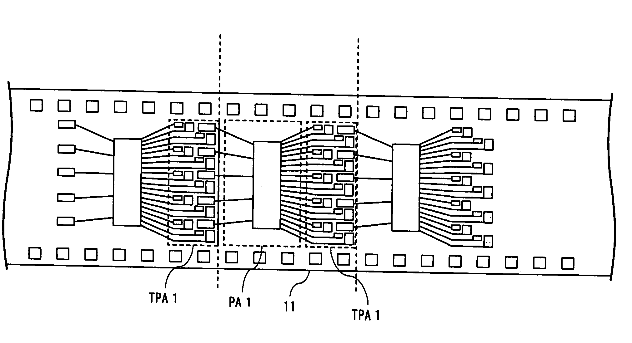
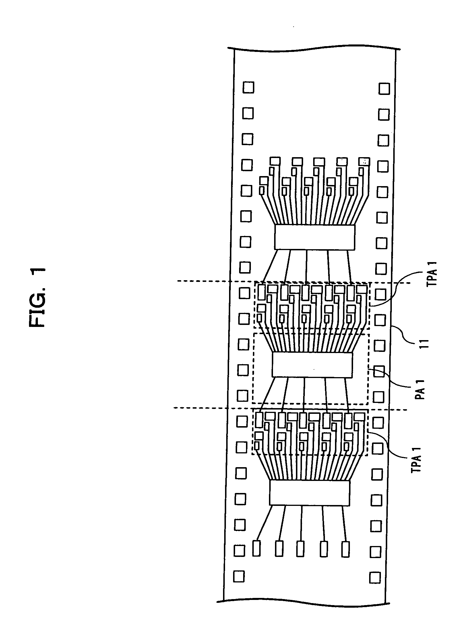
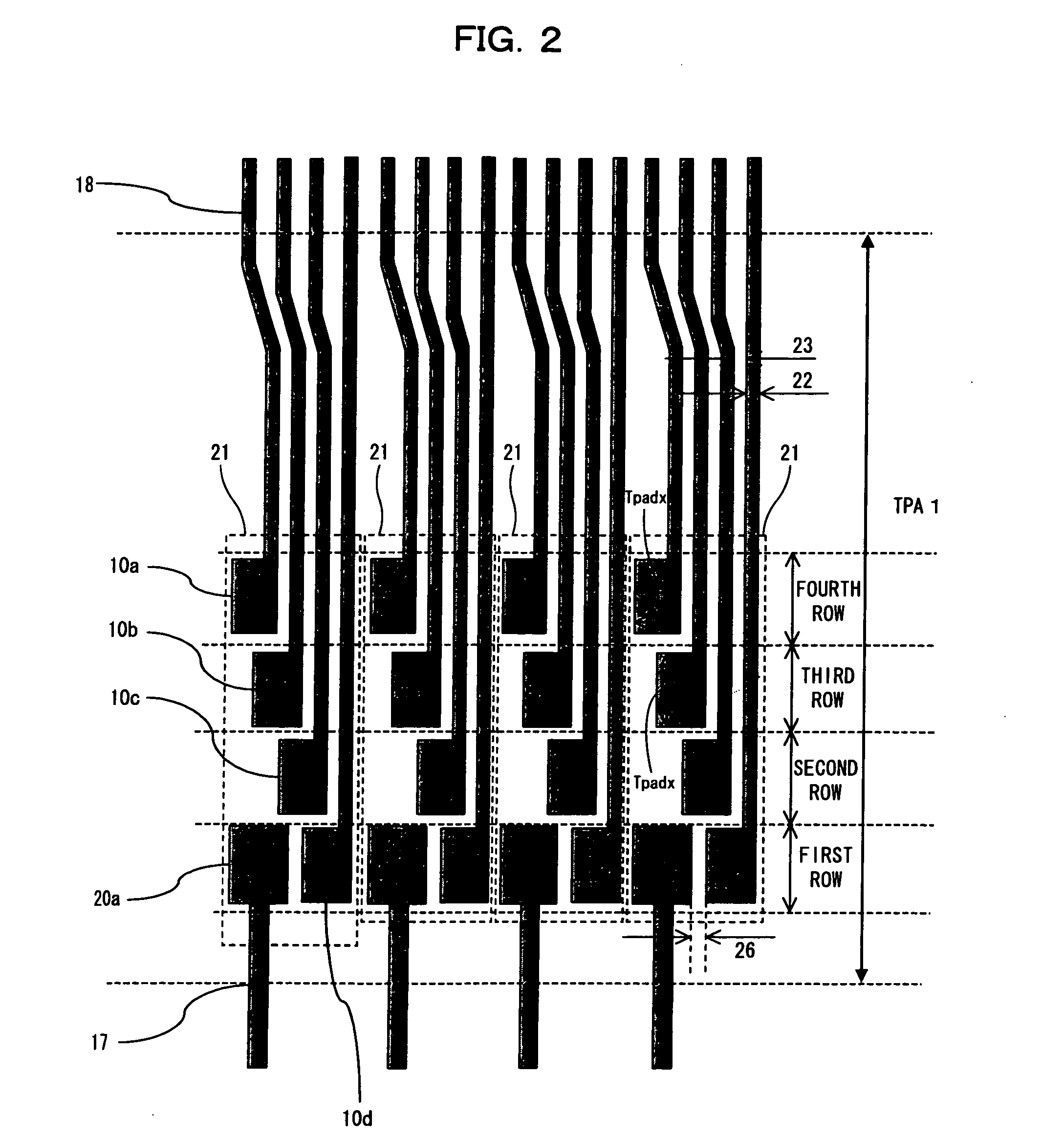
[0043]FIG. 1 is a structural diagram showing the TAP tape of the present invention. FIG. 2 is an enlarged view of a principle part for explaining a test pad area on the TAB tape of the present invention, and an enlarged plan view showing the layout of input / output test pads in an output test pad area TPA1 of FIG. 1. FIG. 3 is a diagram showing a TCP on the TAP tape of the present invention.

[0044] In FIGS. 1 and 2, a TAB tape 11 for TCPs of the present invention has a wiring pattern formed by patterning copper foil on a polyimide base film. The TAB tape 11 comprises package areas PA1 where semiconductor packages are formed and input / output test pad areas TPA1 which are formed on both sides of the package area PA1. Pattern areas are sequentially c...


PUM


Abstract

Input test pads of an adjacent pattern area are placed in a vacant area of a layout area of output test pads, optimizing the layout area of test pads for use in inspection of a semiconductor chip. Thus, it is possible to miniaturize a semiconductor package.

Description

FIELD OF THE INVENTION [0001] The present invention relates to a TAB tape used for a tape carrier package for mounting a semiconductor integrated circuit device and used for a semiconductor package such as a chip on film, and relates to a method of manufacturing the TAB tape. BACKGROUND OF THE INVENTION [0002] In tape automated bonding (TAB), the pads of an IC and the leads of a tape are simultaneously connected with all pins according to tape assembly bonding, thereby achieving quite high connecting efficiency for an IC having multiple pins. A TAB package is called a tape carrier package (TCP) and characterized by a small size, a small thickness, and a light weight. A tape used for TAB is called a tape carrier (film carrier). Further, the sprocket holes of a tape and its associated standards are based on American film standards. The manufacturing process of three-layer tapes started from a 350-μm pitch and 40 pins (calculator) and has become finer year by year. The appearance of a ...

Claims


Application Information

Patent Timeline
IPC IPC(8): G01R31/26
CPCG01R31/2893H01L22/32H01L23/49838H01L23/4985H05K1/0268H01L2924/0002H01L2924/00
Inventor HIRAE, KOUICHI
Owner PANASONIC SEMICON SOLUTIONS CO LTD
Features
  • Generate Ideas
  • Intellectual Property
  • Life Sciences
  • Materials
  • Tech Scout
  • Unparalleled Data Quality
  • Higher Quality Content
  • 60% Fewer Hallucinations
Learn More