Placement configuration of MIM type capacitance element

a capacitance element and placement configuration technology, applied in the direction of fixed capacitor details, fixed capacitors, instruments, etc., can solve the problems of large parasitic resistance, increased parasitic capacitance, and failure to maintain constant parasitic capacitance with respect to voltage, so as to improve relative precision, alleviate the effect of local electrical field concentration and improving relative precision

Active Publication Date: 2006-08-17
PANNOVA SEMIC
View PDF4 Cites 20 Cited by
  • Summary
  • Abstract
  • Description
  • Claims
  • Application Information

AI Technical Summary

Benefits of technology

[0016] Therefore, according to the present invention, a first dummy capacitance element is placed between the first and second capacitance elements respectively adjacent to each other along a direction diagonally intersecting with a direction in parallel with the respective groups of first and second capacitance elements. Further, the interval between the adjacent first and second capacitance elements, an interval between the first capacitance element and the first dummy capacitance element adjacent to each other, and an interval between the second capacitance element and the first dummy capacitance element adjacent to each other are all equalized. Thereby, the parasitic capacitance generated between the capacitance elements, the parasitic capacitance generated between the capacitance element and the peripheral circuit element, and the deterioration of the relative precision resulting from the variation generated in processing the upper electrodes can be controlled.
[0017] According to the placement configuration of the MIM type capacitance elements of the present invention, the deterioration of the relative precision

Problems solved by technology

One of the problems is that there is a large parasitic resistance because an impurity diffusive layer or a conductive poly-Si film in a supported substrate is used in one or both of the electrodes.
The next problem is that a parasitic capacitance is increased because a distance by which the electrode and Si substrate are isolated from each other is approximately not more than a thickness of an insulation film for isolating the elements.
Further, because a depletion layer in the Si substrate changes in response to an applied voltage, a v

Method used


Image

  • Placement configuration of MIM type capacitance element
  • Placement configuration of MIM type capacitance element
  • Placement configuration of MIM type capacitance element

Examples


embodiment 1

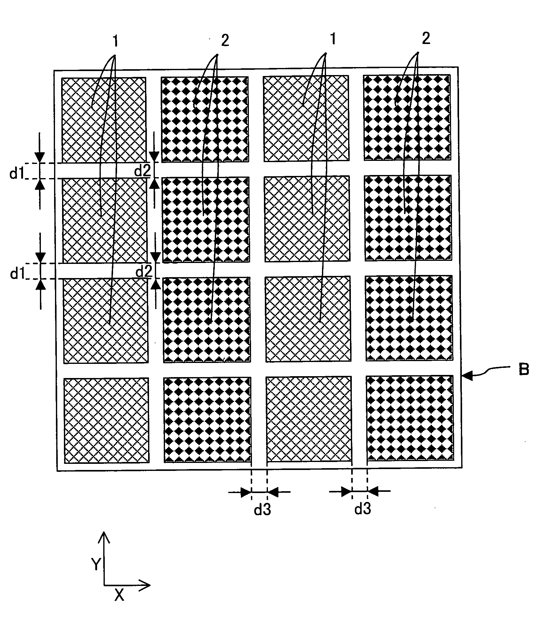
[0031] A first embodiment of the present invention is described referring to FIG. 1. FIG. 1 is a plan view illustrating a placement configuration of MIM type capacitance elements in a supported substrate B such as a silicon (Si) substrate or the like. The capacitance element, which is recited in the description of the present and other embodiments, basically denotes the MIM (Metal Insulator Metal) type capacitance element.

[0032] Reference numerals 1 and 2 shown in FIG. 1 respectively denote a first capacitance element and a second capacitance element. The first and second capacitance elements 1 and 2 are different capacitance elements having an identical capacitance value, which are manufactured by means of a conventional manufacturing method currently available.

[0033] In the present embodiment, groups in which the first capacitance elements 1 are adjacent to one another in a row direction (Y direction), that is, placed in tandem, and groups in which the second capacitance element...

embodiment 2

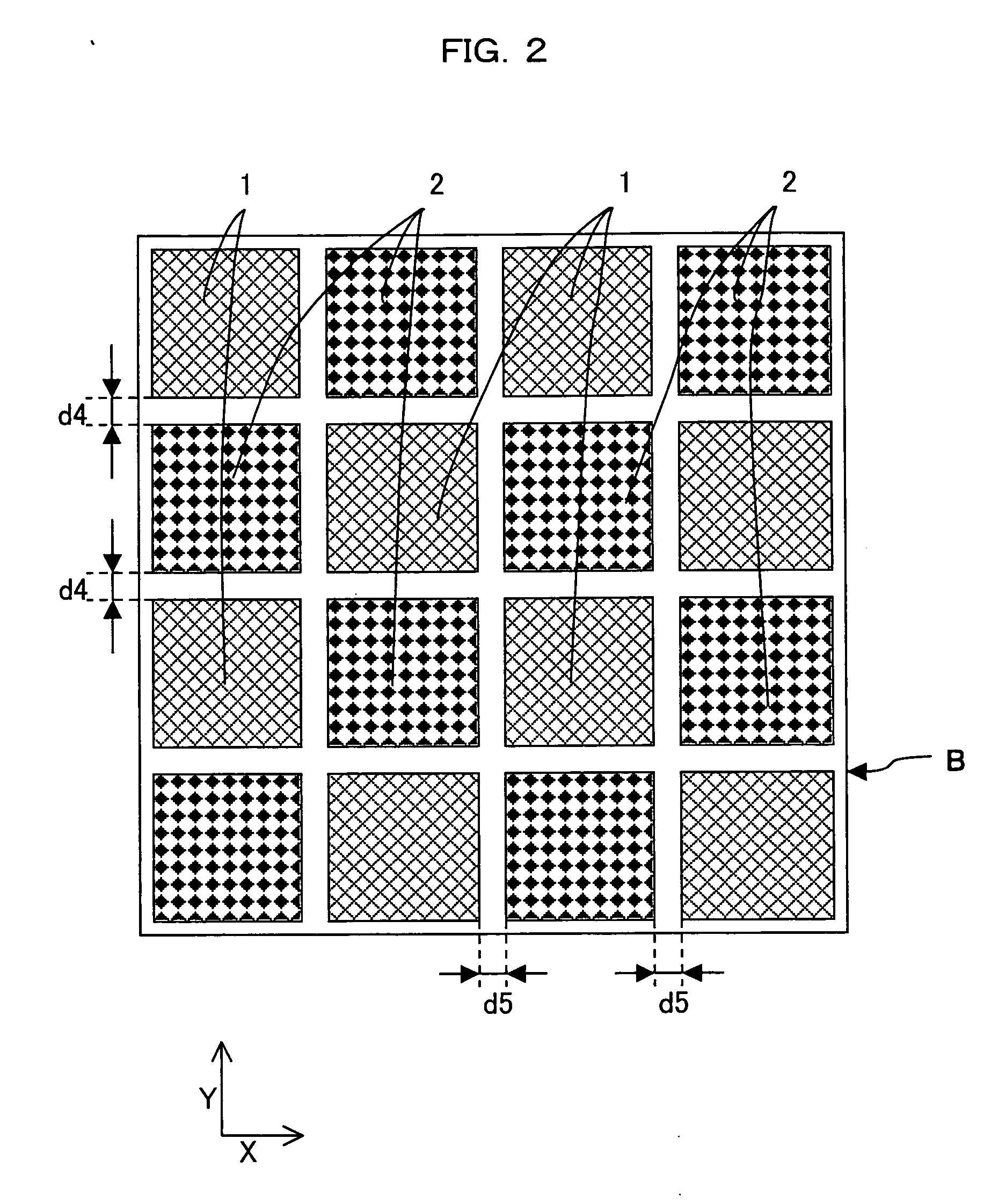
[0041] A second embodiment of the present invention is described referring to FIG. 2. FIG. 2 is a plan view illustrating a placement configuration of MIM type capacitance elements in a supported substrate B such as a silicon (Si) substrate or the like. Reference numerals 1 and 2 shown in FIG. 2 respectively denote a first capacitance element and a second capacitance element. The first and second capacitance elements 1 and 2 are different capacitance elements having an identical capacitance value, which are manufactured by means of a conventional manufacturing method currently available.

[0042] In the present embodiment, the first capacitance elements 1 and the second capacitance elements 2 are alternately placed along both of the row and column directions. Thereby, the first and second capacitance elements 1 and 2 are placed in a grid pattern along the row and column directions, in other words, placed in an array pattern. Further, the first and second capacitance elements 1 and 2 ar...

embodiment 3

[0047] A third embodiment of the present invention is described referring to FIG. 3. FIG. 3 is a plan view illustrating a placement configuration of MIM type capacitance elements. Reference numerals 1′ and 2′ shown in FIG. 3 respectively denote a first capacitance element and a second capacitance element.

[0048] A basic constitution according to the present embodiment is the same as described in the second embodiment. The first and second capacitance elements 1′ and 2′ are alternately placed not only in the row direction but also in the column direction to thereby constitute the array pattern. An interval d6 between the first and second capacitance elements 1′ and 2′ in the row direction and an interval d7 between the first and second capacitance elements 1′ and 2′ in the column direction are equal (d6=d7).

[0049] The present embodiment is characterized in that corners of the first and second capacitance elements 1′ and 2′ have an obtuse angle, in other words, shapes of the first an...


PUM


Abstract

A placement configuration of MIM type capacitance elements according to the present invention comprises a group of first capacitance elements in which the first capacitance elements as the MIM type capacitance elements are placed in tandem and a group of second capacitance elements in which the second capacitance elements as the MIM type capacitance elements are placed in tandem, wherein the group of first capacitance elements and the group of second capacitance elements are alternately placed in parallel with each other with an equal interval therebetween.

Description

BACKGROUND OF THE INVENTION [0001] 1. Field of the Invention [0002] The present invention relates to a placement configuration of an electrostatic capacitance element having a metal—insulation film—metal (MIM) structure, more particularly to a placement configuration of two MIM type capacitance elements having an identical capacitance value. [0003] 2. Description of the Related Art [0004] An analog integrated circuit used in a mobile communication device such as a cellular telephone is provided with passive elements such as a capacitance element, a resistance and an inductor. As the capacitance element among the passive elements, which is particularly frequently used in an operational amplifier of a pipeline-type A / D converter, two capacitance elements having an identical capacitance value are used in order to eliminate any error generated in the A / D conversion, and a high relative precision is demanded between the two capacitance elements. The relative precision refers to a differe...

Claims


Application Information

Patent Timeline
IPC IPC(8): G02F1/136
CPCH01L27/0207H01L27/0805
Inventor NABESHIMA, YUTAKA
Owner PANNOVA SEMIC
Why Eureka
Try Eureka