Method of forming film pattern, method of manufacturing device, electro-optical device, and electronic apparatus

a manufacturing method and film pattern technology, applied in the direction of photomechanical treatment originals, identification means, instruments, etc., can solve the problems of high production cost and waste of materials, insufficient adhesion between the pattern and the substrate, and inability to form a highly reliable device, so as to prevent the occurrence of a pattern or a pattern. wettability. the effect of forming the pattern

Inactive Publication Date: 2006-08-17
SEIKO EPSON CORP
View PDF3 Cites 11 Cited by
  • Summary
  • Abstract
  • Description
  • Claims
  • Application Information

AI Technical Summary

Benefits of technology

[0008] An advantage of some aspects of the invention is that it provides a method of forming a film pattern which is capable of consistently forming a fine film pattern with high performance, a device, a method of manufacturing a device, an electro-optical device, and an electronic apparatus.
[0010] According to the invention, since the forming of the irregularities between the banks is conducted, the lyophilic property of a surface of the substrate is improved, and thus the functional liquid can be uniformly disposed on the substrate. In addition, due to the irregularities formed on the surface of the substrate, the contact area between the substrate and the film is increased, which improves the adhesion of the film. In addition, since the functional liquid for forming the film pattern is disposed between the banks formed on the substrate, it is possible to prevent the functional liquid from scattering around liquid droplets and to easily form the wiring pattern in a predetermined shape according to the shape of the banks.
[0012] According to the method, it is possible to easily form the minute irregularities on the surface of the substrate. In addition, by fluorinating the banks before forming the irregularities, the banks can have corrosion resistance with respect to an etchant.
[0015] According to the method, it is possible to obtain the device having the film pattern which is reliably adhered to the substrate and is capable of preventing the occurrence of a problem, such as circuit shortage.
[0017] According to the invention, it is possible to obtain the electro-optical device and an electronic apparatus each of which has the film pattern capable of preventing the occurrence of a problem, such as circuit shortage.

Problems solved by technology

However, the photolithography method requires large-size equipment, such as a vacuum apparatus, or a complicated process, and only a small percentage of the materials are used, causing high production cost and waste of materials.
However, there is the following problem in the conventional method described above.
When a functional liquid is disposed on the substrate so as to form a wiring pattern, if the substrate has not been subjected to any treatment, there is a possibility that the wettability required to form the pattern or the adhesion between the pattern and the substrate will be insufficient.
For this reason, when a fine pattern is formed, some wiring lines are short-circuited, which does not allow a highly reliable device to be formed.

Method used


Image

  • Method of forming film pattern, method of manufacturing device, electro-optical device, and electronic apparatus
  • Method of forming film pattern, method of manufacturing device, electro-optical device, and electronic apparatus
  • Method of forming film pattern, method of manufacturing device, electro-optical device, and electronic apparatus

Examples


Embodiment Construction

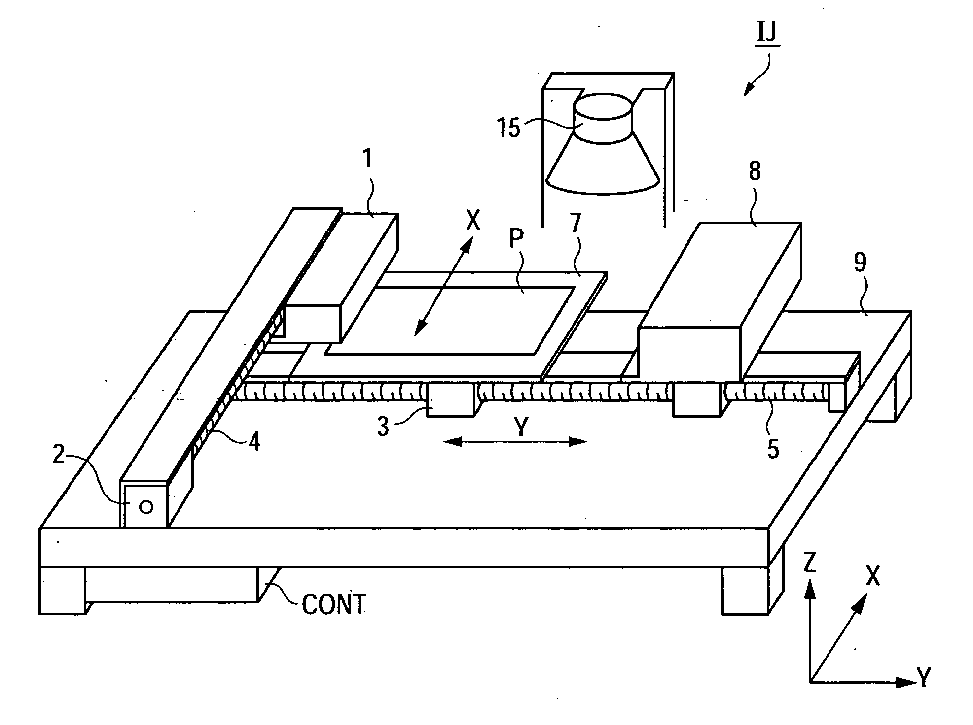
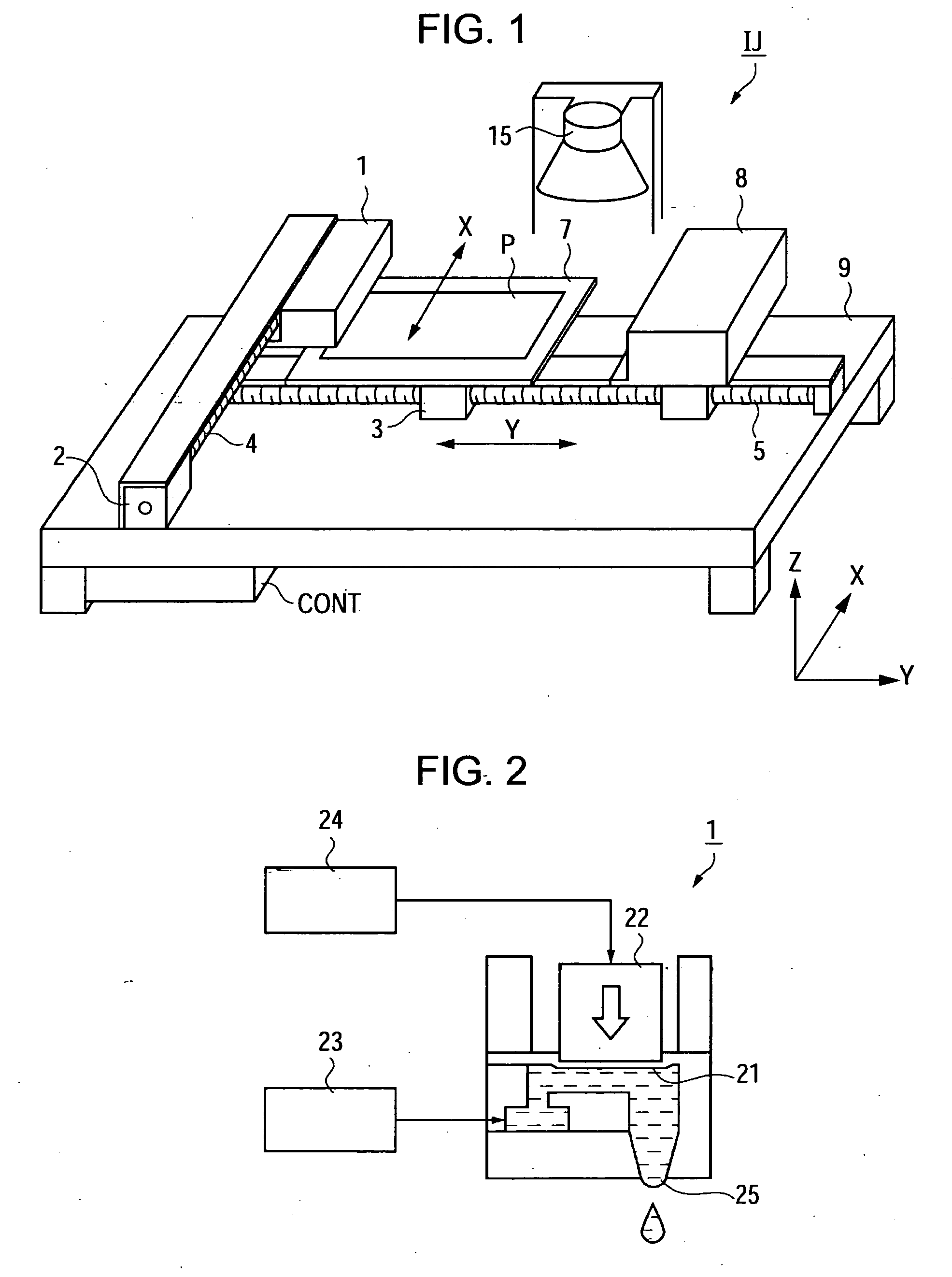
[0031] Hereinafter, a method of forming a film pattern and a method of manufacturing a device according to an embodiment of the invention will be described with reference to the accompanying drawings. In the embodiment, a case will be described as an example in which wiring pattern forming ink is discharged from discharging nozzles of a liquid droplet discharging head in the shape of liquid droplets by using a liquid droplet discharging method, the wiring pattern forming ink including a material which has conductivity by, for example, heat treatment, and thus a wiring pattern (film pattern) composed of a conductive film is formed.

[0032] First, an ink to be used will be described. The ink corresponds to functional liquid of the invention. The functional liquid refers to solution capable of forming a film (functional film) having a specific function by making film components contained in liquid formed as a film. As the function, there are various functions such as electrical and elec...


PUM

PropertyMeasurementUnit
diametersaaaaaaaaaa
diametersaaaaaaaaaa
diametersaaaaaaaaaa

Abstract

A method of forming a film pattern by disposing a functional liquid on a substrate includes: forming banks corresponding to the film pattern on the substrate; forming irregularities on bottoms between the banks by using the banks as a mask; and disposing the functional liquid between the banks and on the bottoms formed with the irregularities.

Description

RELATED APPLICATIONS [0001] This application claims priority to Japanese Patent Application Nos. 2005-040126 filed Feb. 17, 2005 and 2005-328485 filed Nov. 14, 2005 which are hereby expressly incorporated by reference herein in their entirety. BACKGROUND [0002] 1. Technical Field [0003] The present invention relates to a method of forming a film pattern, a method of manufacturing the device, an electro-optical device, and an electronic apparatus. [0004] 2. Related Art [0005] Devices having wiring lines, such as electronic circuits or integrated circuits, are manufactured by using a photolithography method, for example. The photolithography method is used to apply a photosensitive material, which is called a resist, on a substrate on which a conductive film is applied beforehand, irradiate and develop a circuit pattern, and etch the conductive film according to a resist pattern so as to form a wiring pattern of a thin film. However, the photolithography method requires large-size equ...

Claims


Application Information

Patent Timeline
Patent Type & Authority Applications(United States)
IPC IPC(8): G03F1/00G02F1/1343G09F9/00
CPCG02B5/201H01L51/0005H01L51/56H05K3/125H05K3/1258H05K3/381H05K2203/013H05K2203/0568H10K71/135H10K71/00A47G1/06
Inventor SAKASHITA, TOMOKIMORIYA, KATSUYUKIHIRAI, TOSHIMITSU
Owner SEIKO EPSON CORP
Why Eureka
Try Eureka