Air void via tuning

a via structure and air gap technology, applied in the field of wiring boards, can solve the problems of increasing the density of the circuit, exacerbate the tuning problem, and the insertion and return loss, and achieve the effect of improving the main contributing factor

Inactive Publication Date: 2006-08-24
SIMCLAR INTERCONNECT TECH
View PDF28 Cites 64 Cited by
  • Summary
  • Abstract
  • Description
  • Claims
  • Application Information

AI Technical Summary

Benefits of technology

[0013] The present invention addresses the problems caused in high-speed digital and RF system design where a number of electrical or electronic components are connected through printed circuit boards (PCB's) and connectors. Specifically, the present invention concerns tuning via structu

Problems solved by technology

While clearly improving signal integrity none of the aforementioned known methods are capable of tuning the differential and single ended via structures to the same degree in terms of impedance, insertion and return loss

Method used


Image

  • Air void via tuning
  • Air void via tuning
  • Air void via tuning

Examples


Embodiment Construction

[0028] So that the manner in which the above recited features, advantages, and objects of the present invention are attained can be understood in detail, more particular description of the invention, briefly summarized above, may be had by reference to the embodiment thereof that is illustrated in the appended drawings. In all the drawings, identical numbers represent the same elements.

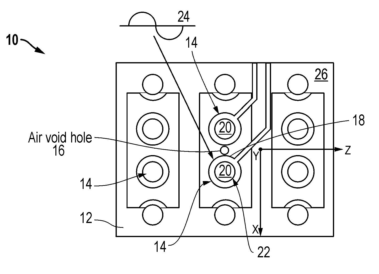
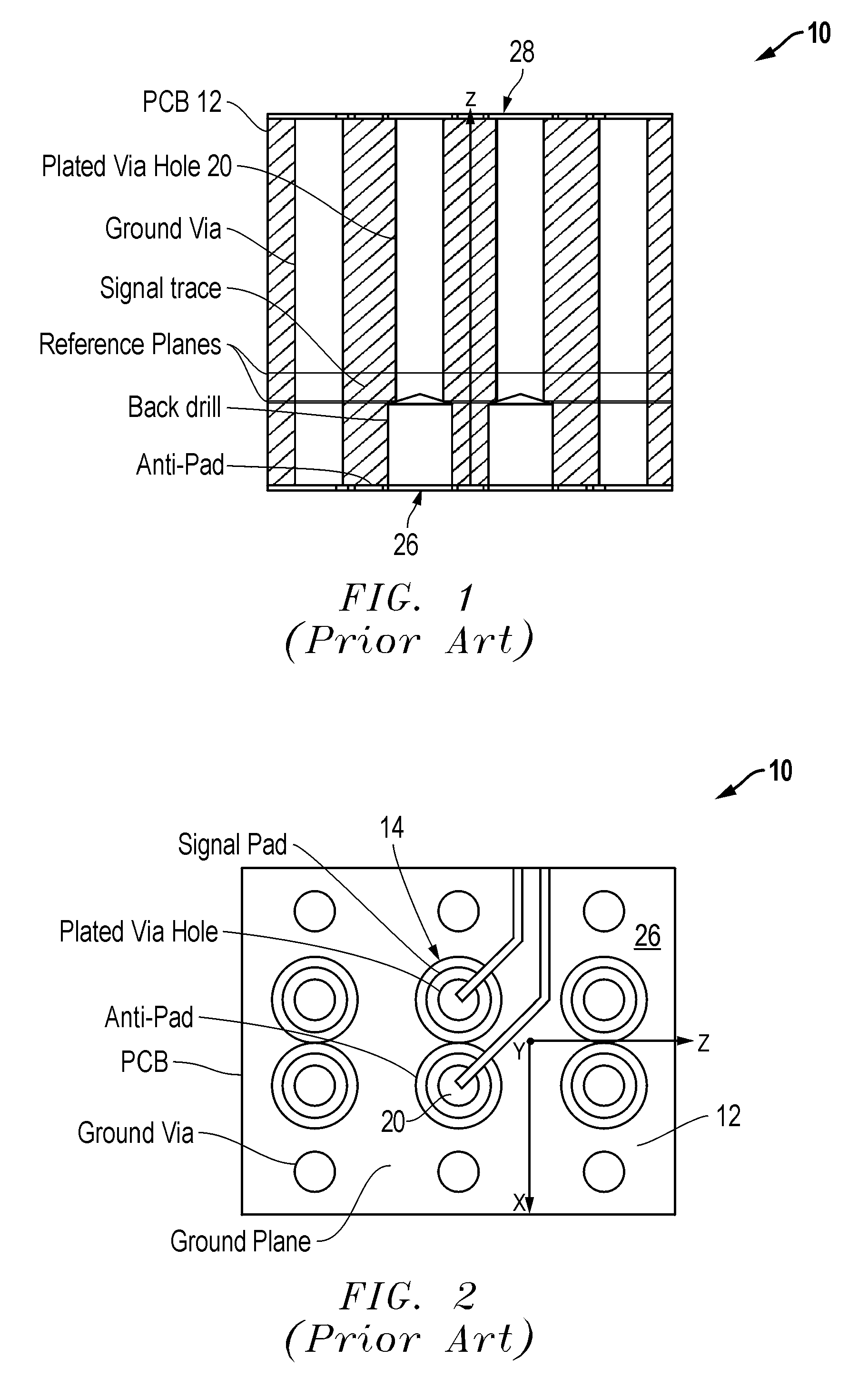
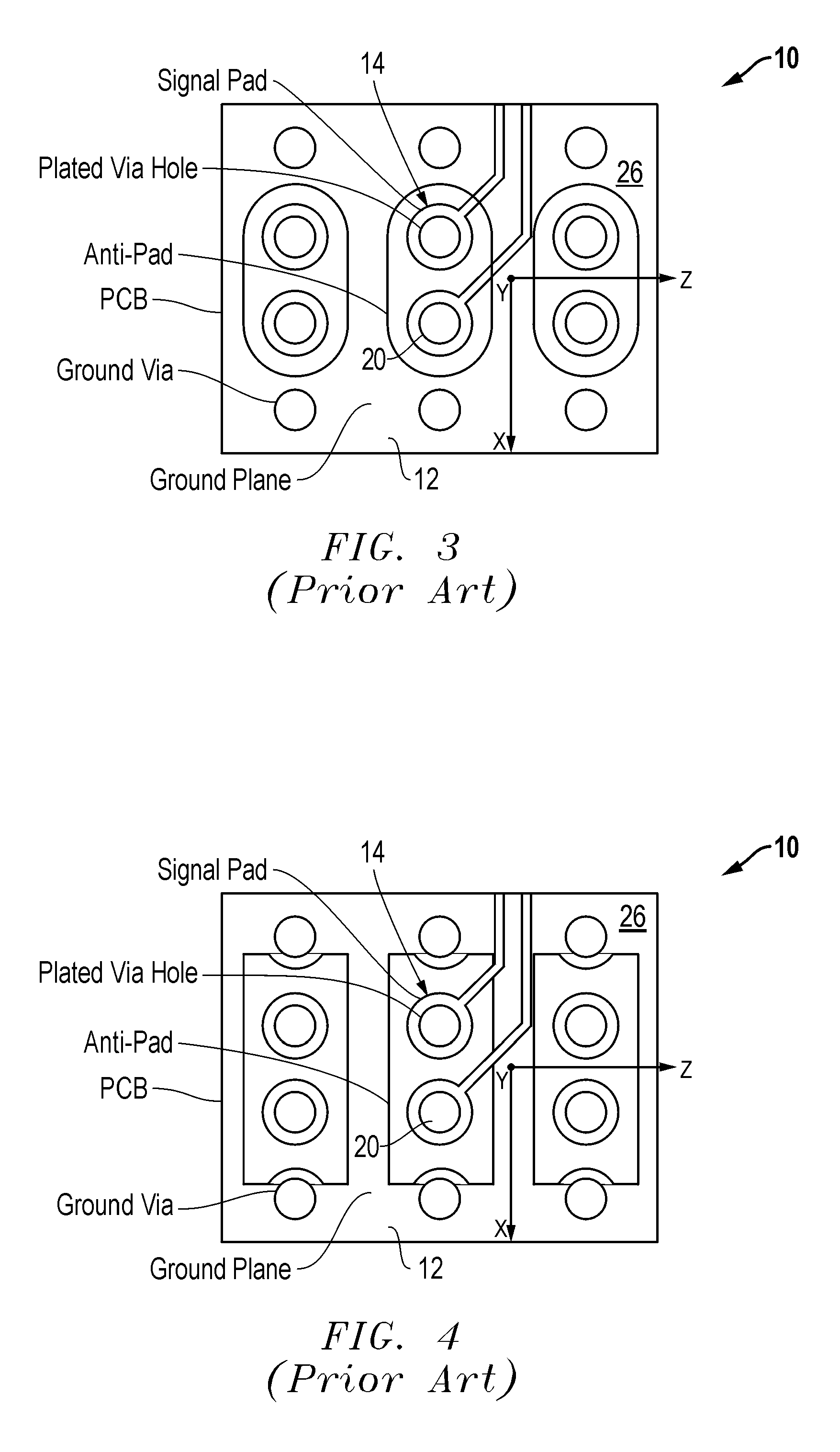
[0029] In the present invention a wiring board 10 and method of manufacture is disclosed. The electronics wiring board 10 having reduced electromagnetic coupling between electronic devices includes a base board 12 that is adaptable to receive at least one electronic component 14 mounted on the base board 12. At least one hole or void 16 is formed in the base board 12 in the proximity of the electronic component 14 to be isolated. The hole 16 is separated from the selected electronic component 14 to be isolated against undesired electromagnetic radiation by a portion or segment 18 of the base board or...


PUM


Abstract

A wiring board (10) having reduced electromagnetic coupling between electronic devices includes a base board (12) that is adaptable to receive at least one electronic component (14) mounted on the base board (12). At least one hole or void (16) is formed in the base board (12). The hole (16) is separated from the selected electronic component (14) to be isolated against undesired electromagnetic radiation by a portion (18) of the base board (12).

Description

BACKGROUND OF THE INVENTION [0001] 1. Technical Field [0002] The invention relates to the field of wiring boards for electronic devices, and more particularly to methods to suppress undesired electromagnetic radiation and coupling in components of the circuitry mounted on or formed with the wiring board. [0003] 2. Background Art [0004] It is known to tune single vias by having a large hole on the upper layers of a base board or Printed Circuit Board (PCB) to accommodate a through hole connector and a narrower hole for the remaining layers to the bottom side. [0005] Back drilling, which is the post process of drilling out the unused portion of the via barrel from the bottom side as close as is practicable to the signal trace, is also a known method used to reduce the effects of stubs on signal integrity. See FIG. 1. [0006] Techniques are also known to address the problems of stray capacitance and creapage and clearance make use of larger clearances or separations between the signal v...

Claims


Application Information

Patent Timeline
IPC IPC(8): H05K1/11
CPCH05K1/0216H05K1/0237H05K1/024H05K1/115H05K1/18H05K2201/0792H05K2201/09063
Inventor ROBINSON, THOMAS RICHARD
Owner SIMCLAR INTERCONNECT TECH
Why Eureka
Try Eureka