Static random access memory (SRAM) compatible, high availability memory array and method employing synchronous dynamic random access memory (DRAM) in conjunction with a single DRAM cache and tag

a dynamic random access memory and synchronous technology, applied in the field of integrated circuit memory devices, to achieve the effect of preventing data loss

Inactive Publication Date: 2006-08-24
UNITED MEMORIES +1
View PDF27 Cites 12 Cited by
  • Summary
  • Abstract
  • Description
  • Claims
  • Application Information

AI Technical Summary

Benefits of technology

[0027] In particular embodiments of the present invention disclosed herein, a synchronous DRAM device, or other integrated circuit device employing embedded SDRAM is provided that incorporates a control logic block, a DRAM cache, a tag, a write-back address counter and specific data and address bussing. In operation and architecture, there is provided, therefore a memory array which is constructed

Problems solved by technology

In contrast, the techniques described in the '474 and '685 patents allows data from any or all subarray

Method used


Image

  • Static random access memory (SRAM) compatible, high availability memory array and method employing synchronous dynamic random access memory (DRAM) in conjunction with a single DRAM cache and tag
  • Static random access memory (SRAM) compatible, high availability memory array and method employing synchronous dynamic random access memory (DRAM) in conjunction with a single DRAM cache and tag
  • Static random access memory (SRAM) compatible, high availability memory array and method employing synchronous dynamic random access memory (DRAM) in conjunction with a single DRAM cache and tag

Examples


Embodiment Construction

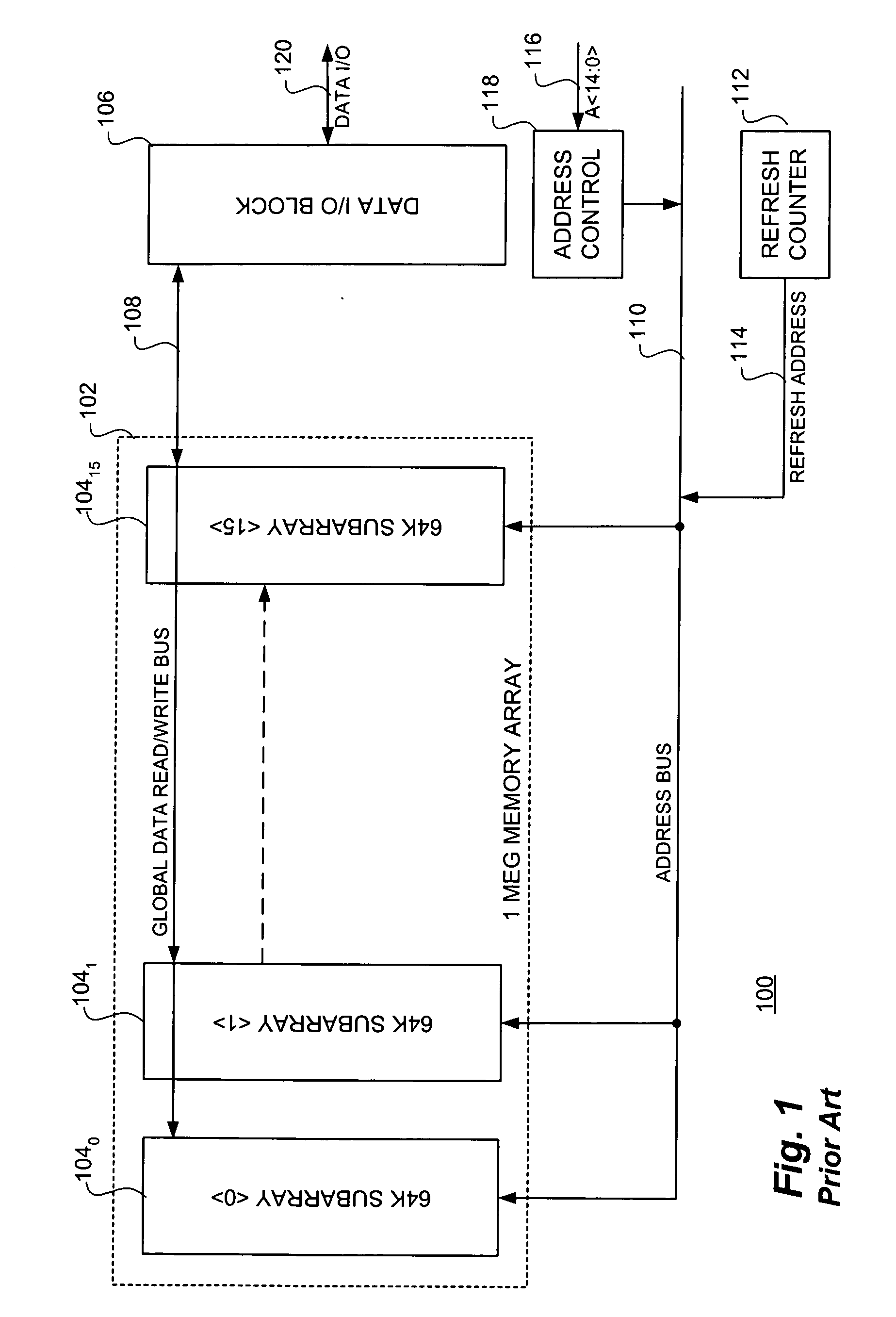
[0044] With reference now to FIG. 1, a functional block diagram of a conventional memory 100 is shown illustrating the data and address bussing thereof and wherein refresh operations are not hidden. The conventional DRAM memory 100 comprises, in pertinent part, a 1 Meg memory array 102 comprising 16 separate 64 K subarrays 1040 through 10415 (subarray 0> through subarray 15>) as illustrated.

[0045] A data input / output (I / O) block 106 is coupled to the various subarrays 1040 through 10415 by means of a global data read / write bus 108. Memory locations within the subarrays 1040 through 10415 are addressed by means of an address bus 110 or a refresh address determined by a refresh counter 112 which provides a refresh address on bus 114 coupled to the address bus 110. Addresses to be read or written within the memory array 102 are input on address bus 116 (A14:0>) for input to an address control block 118, which is, in turn, coupled to the address bus 110. Data read from, or to be writte...


PUM


Abstract

A static random access memory (SRAM) compatible, high availability memory array and method employing synchronous dynamic random access memory (DRAM) in conjunction with a single DRAM cache and tag provides a memory architecture comprising low cost DRAM memory cells that is available for system accesses 100% of the time and is capable of executing refreshes frequently enough to prevent data loss. Any subarray of the memory can be written from cache or refreshed at the same time any other subarray is read or written externally.

Description

BACKGROUND OF THE INVENTION [0001] The present invention relates, in general, to the field of integrated circuit memory devices and those devices incorporating embedded memory. More particularly, the present invention relates to a static random access memory (SRAM) compatible, high availability memory array and method employing synchronous dynamic random access memory (DRAM) in conjunction with a single DRAM cache and tag, hereinafter sometimes referred to as SCRAM (SRAM Compatible Random Access Memory). [0002] SRAM is a type of memory technology which can maintain data without needing to be refreshed for as long as power is supplied to the circuit (i.e. “static”). This is, in contrast to DRAM which must be refreshed many times per second in order to maintain its data (i.e. “dynamic”). Among the main advantages of SRAM over DRAM is the fact that the former doesn't require refresh circuitry in order for it to maintain data, unlike the latter. For this and other reasons, the data acce...

Claims


Application Information

Patent Timeline
IPC IPC(8): G06F13/28
CPCG06F12/0893G06F2212/3042G11C11/406G11C11/40603G11C11/40607G11C11/40615G11C11/40618
Inventor BUTLER, DOUGLAS BLAINEJONES, OSCAR FREDERICK JR.PARRIS, MICHAEL C.
Owner UNITED MEMORIES
Why Eureka
Try Eureka