
Apparatus and method for processing wafer

a technology of etching technique and semiconductor wafer, which is applied in the direction of ohmic resistance heating, hot plate heating arrangement, coating, etc., can solve the problems of vital importance in temperature control of semiconductor wafer during processing, poor reproducibility of etching results without temperature, and the inability to achieve the most uniform cd distribution of semiconductor wafers

Inactive Publication Date: 2006-08-31
HITACHI HIGH-TECH CORP
View PDF9 Cites 19 Cited by
  • Summary
  • Abstract
  • Description
  • Claims
  • Application Information

AI Technical Summary

Benefits of technology

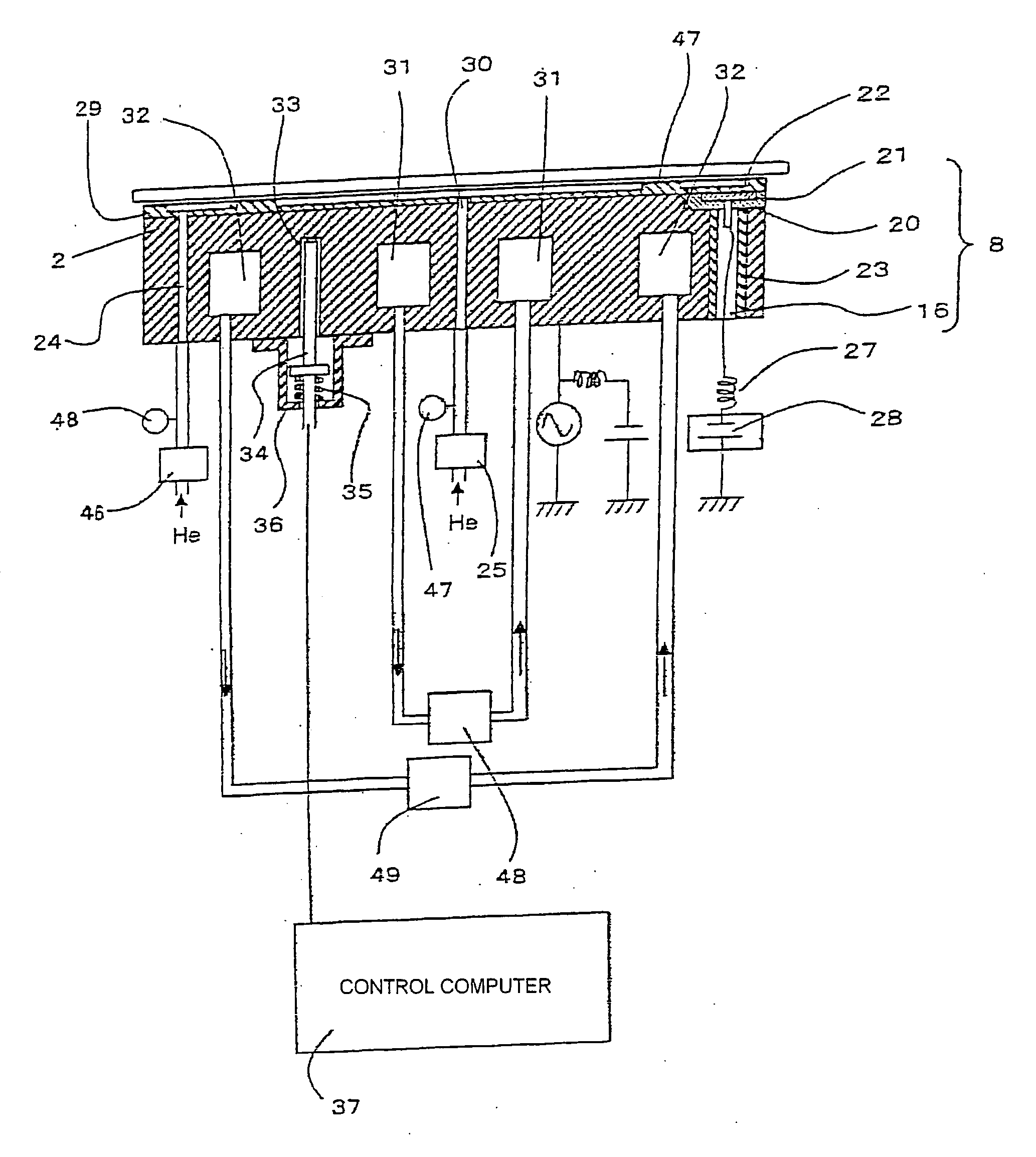
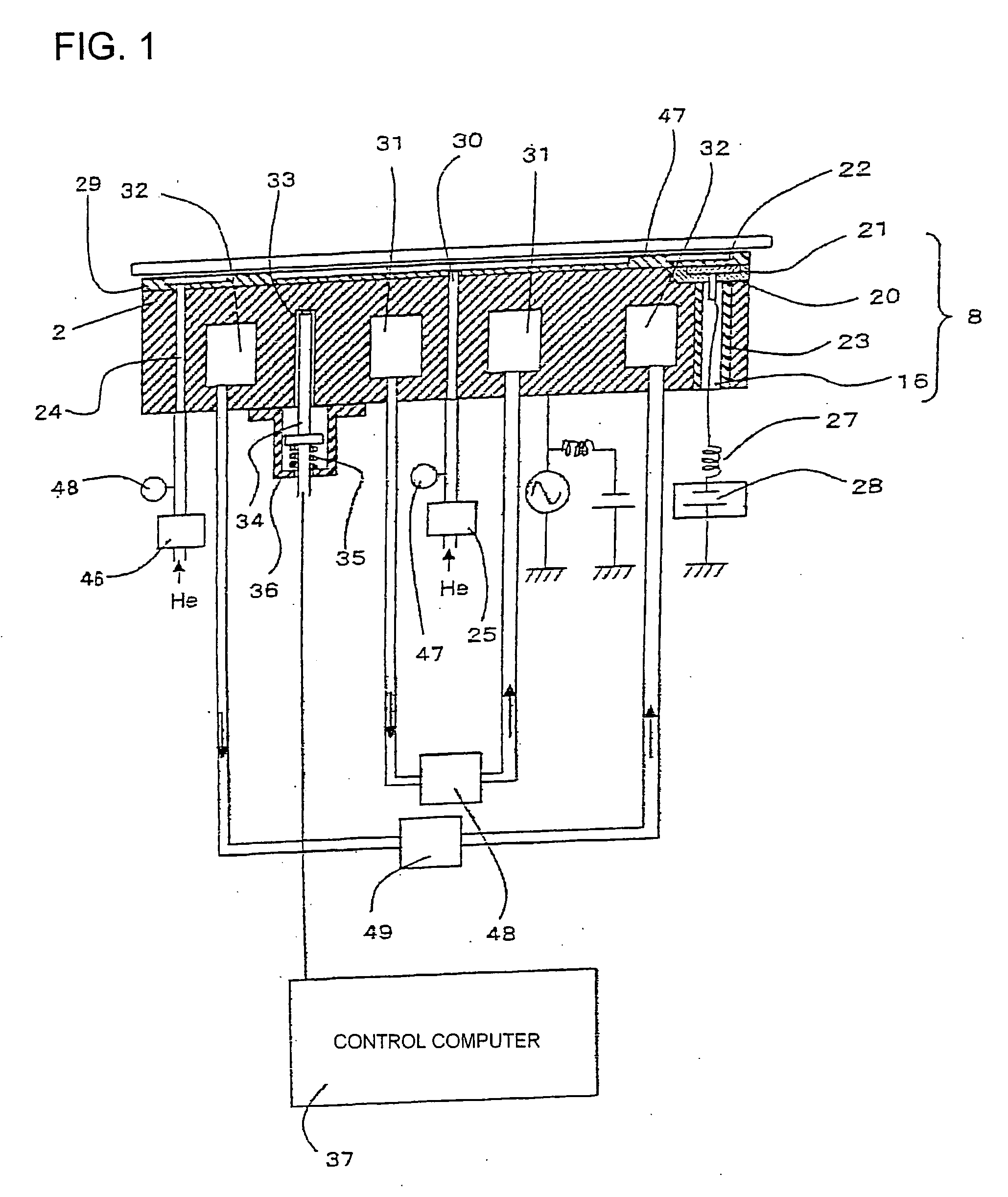
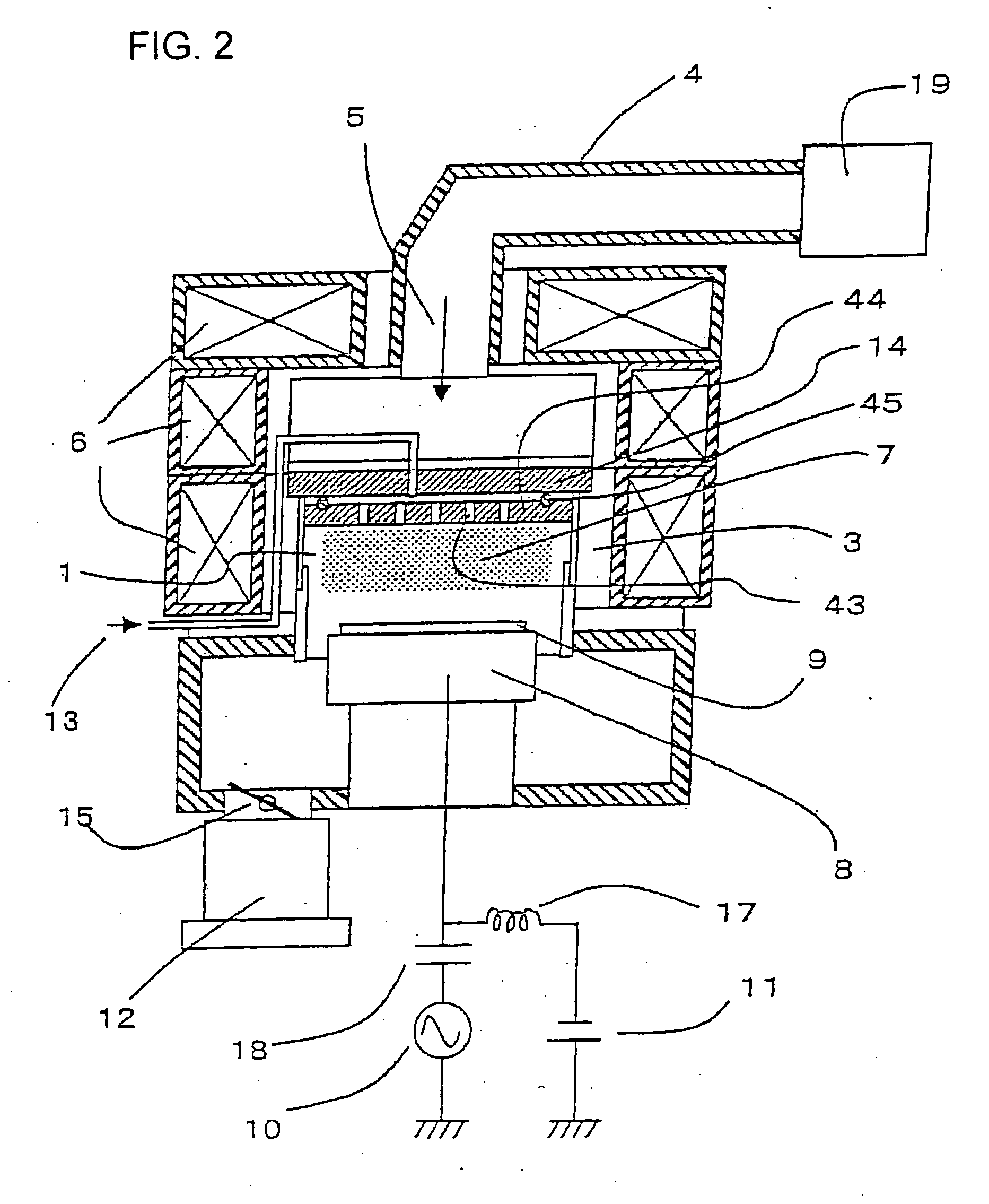
The invention provides a wafer processing apparatus and method with reduced within-wafer dimensional variation. This is achieved by regulating the temperature of the semiconductor wafer or the heat transfer coefficient between the wafer and the wafer stage through various means such as circulating temperature regulating agent or cooling gas pressure. The control computer can also receive input of CD measurements for processes in different temperature conditions to determine the optimal temperature condition for achieving a uniform CD distribution within the wafer. This invention allows for the achievement of a uniform CD distribution within the wafer and ensures high processing efficiency for different kinds of films.

Problems solved by technology

In this situation, temperature control of a semiconductor wafer during processing is a problem of vital importance.
Hence the etching result will have poor reproducibility without temperature control of the wafer during processing.
Conventionally, however, the temperature distribution of a semiconductor wafer achieving the most uniform CD distribution within a wafer cannot be easily obtained.
There is no control for regulating the within-wafer temperature distribution in response to the change of etching condition.
A problem in the above-described conventional art is the difficulty of etching with the temperature distribution that results in the smallest within-wafer dimensional variation after etching.
Another problem is that, under step-by-step changing etching conditions, such as in sequential processing for different kinds of films, a temperature distribution capable of reducing dimensional variation cannot be used for each particular etching condition, which makes it difficult to achieve a uniform etching result.

Method used


Image

  • Apparatus and method for processing wafer
  • Apparatus and method for processing wafer
  • Apparatus and method for processing wafer

Examples


first embodiment

[0041] With reference to the flow chart of FIG. 4, a process flow for determining the etching condition is described, which is a feature of the invention. First, the etching process is performed N times in different temperature conditions of the semiconductor wafer, and the CD shift for each etching iteration is measured (101). Here, in order to reveal the relationship between the wafer temperature and the CD shift, it is desirable that process conditions other than temperature such as gas species, flow rate, pressure, source power, and bias power be identical. These conditions can be determined on the basis of past experiences and results. However, they may be different from the final conditions. If so, the same procedure will be carried out in the modified conditions.

[0042] The CD shift data obtained from this experiment is inputted to the control computer (102). The control computer determines a relationship equation between the CD shift and the wafer temperature (103). The wafer...

second embodiment

[0061] the invention is useful because the temperature for each step is regulated to a temperature that provides a uniform within-wafer CD distribution. However, the temperature control may be insufficient for processes of interest that are very sensitive to temperature. For example, the wafer is not at a temperature that provides a uniform within-wafer CD distribution after the step is switched and until the temperature distribution reaches the optimal distribution. Therefore, during this period of time, the CD distribution may be varied. Moreover, if the switched step requires complete replacement of process gas, which lasts several tens of seconds, the temperature of the wafer heated in the preceding step will gradually decrease. This will extend, in the next step, the time required for reaching the optimal wafer temperature that provides a uniform within-wafer CD distribution.

[0062] In this regard, the third embodiment of the invention to solve the above problem will be describe...

fourth embodiment

[0066] Next, with reference to FIG. 13, the fourth embodiment is described, which is directed to a processing method that can further improve manufacturing yield when the embodiment of the invention is applied to an actual semiconductor production line. This embodiment is effective in the case where increase of processed wafers in an actual production line results in deposits of reaction products adhered to the inner wall of the vacuum chamber, for example, and reaction products are supplied from the deposits. That is, when the within-wafer CD distribution obtained for the process condition determined from measurements of the original CD distribution is gradually changed by reaction products supplied from the wall, the within-wafer CD distribution is measured each time a predetermined cumulative number of wafers are processed. The process condition is determined again on the basis of this result.

[0067] First, the process condition is determined-according to the first embodiment (401...


PUM

PropertyMeasurementUnit
temperatureaaaaaaaaaa
pressureaaaaaaaaaa
input poweraaaaaaaaaa

Abstract

A wafer processing apparatus capable of obtaining a uniform CD distribution within a wafer is provided. The wafer processing apparatus comprises at least two separate circuits of temperature regulating means provided in a wafer stage, a plurality of cooling gas pressure regulating means for feeding cooling gas between the semiconductor wafer and the wafer stage, means for regulating heater input power, and a control computer. The control computer receives input of line width dimensions resulting from processes in an arbitrary plurality of temperature conditions obtained by changing at least one of the conditions of the temperature of the temperature regulating agent, the cooling gas pressure, and the input power of the heater. The line width dimensions are used to calculate, and control, at least one of the temperature of the temperature regulating agent, the cooling gas pressure, and the input power of the heater for obtaining an arbitrary etching line width dimension.

Description

[0001] The present application is based on and claims priority of Japanese patent application No. 2005-028804 filed on Feb. 4, 2005, the entire contents of which are hereby incorporated by reference. BACKGROUND OF THE INVENTION [0002] 1. Field of the Invention [0003] The invention relates to an etching technique for a semiconductor wafer, and more particularly to a wafer processing apparatus and a wafer processing method with reduced dimensional variation within a semiconductor wafer. [0004] 2. Description of the Related Art [0005] In recent years, circuit patterns processed on a semiconductor wafer continue to shrink with the trend toward higher integration of semiconductor devices, which requires increasingly higher accuracy of processing dimension. In this situation, temperature control of a semiconductor wafer during processing is a problem of vital importance. [0006] For example, when a semiconductor wafer is etched with plasma, typically, a bias voltage is applied to the semic...

Claims


Application Information

Patent Timeline
Patent Type & Authority Applications(United States)
IPC IPC(8): C23C16/00
CPCH01J37/32935H01J37/3299H01J2237/2001H01L21/32137H01L21/67069H01L21/67109
Inventor KANNO, SEIICHIROTANAKA, JUNICHIMIYA, GOTSUBONE, TSUNEHIKOMAKINO, AKITAKAMASUDA, TOSHIO
Owner HITACHI HIGH-TECH CORP
Learn More