Pattern transferring mold, pattern transferring apparatus and device manufacturing method using the same

Inactive Publication Date: 2006-08-31
CANON KK
View PDF3 Cites 40 Cited by
  • Summary
  • Abstract
  • Description
  • Claims
  • Application Information

AI Technical Summary

Benefits of technology

[0011] One object of the present invention is to provide a pattern transferring mold which can provide

Problems solved by technology

Therefore, a long time to release the mold from the substrate (hereinafter, it is referred to as mol

Method used


Image

  • Pattern transferring mold, pattern transferring apparatus and device manufacturing method using the same
  • Pattern transferring mold, pattern transferring apparatus and device manufacturing method using the same
  • Pattern transferring mold, pattern transferring apparatus and device manufacturing method using the same

Examples


embodiment 1

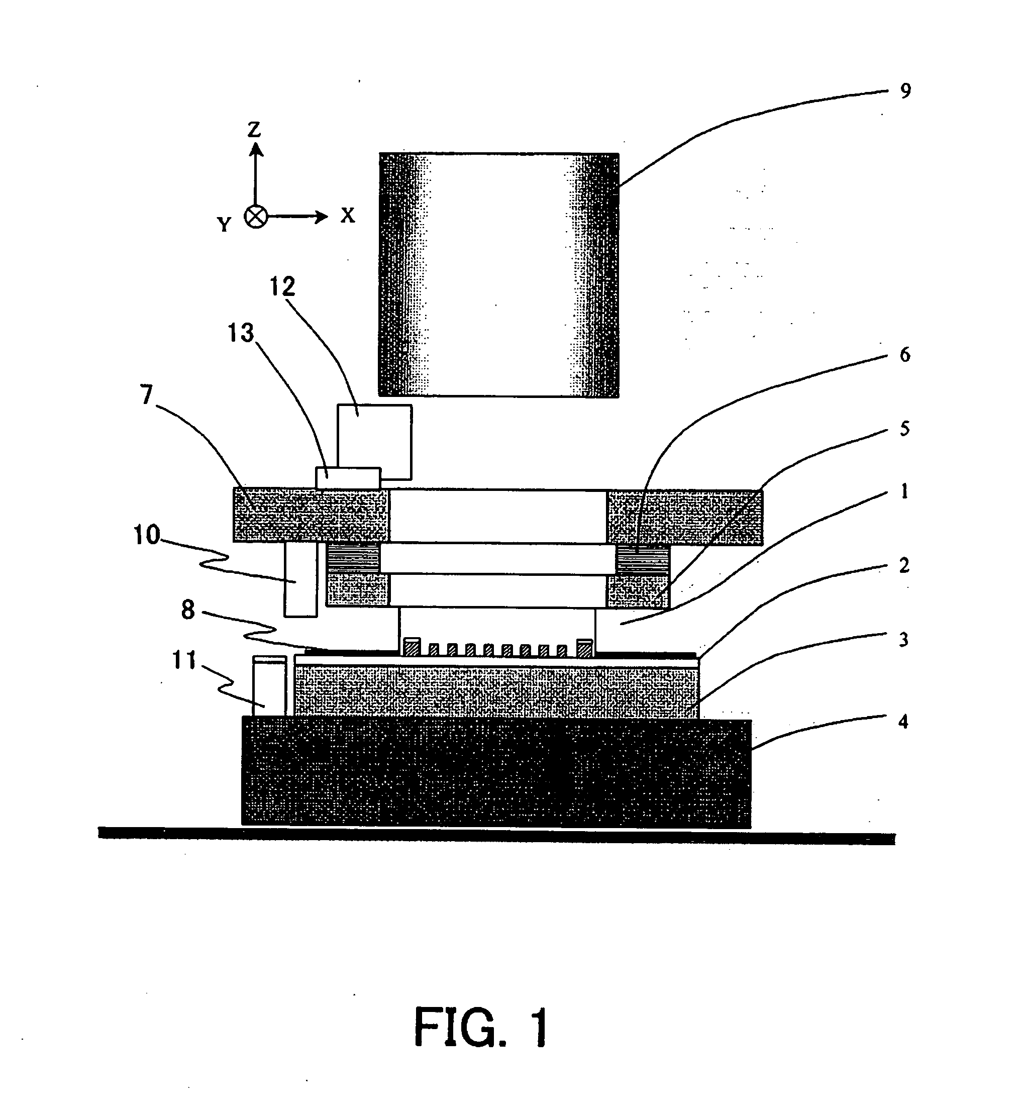
[0027]FIG. 1 shows a photo-curing type (or UV-curing type) nanoimprint apparatus (or pattern transferring apparatus) in schematic form, which uses a pattern transferring mold that is Embodiment 1.

[0028] In FIG. 1, 1 denotes a pattern transferring mold (original plate or a template) having a relief pattern for semiconductor devices such as a large-scale integrated circuit and MEMS. 2 denotes a wafer that is a substrate, and 3 denotes a wafer chuck for holding the wafer 2. 4 denotes a wafer stage for positioning the wafer 2. The wafer stage 4 can perform X, Y and Z axes directional driving and rotational driving (ωx, ωy, and θ) around each axis.

[0029]5 denotes a mold chuck for holding the mold 1, and 6 denotes a mold stage for positioning the mold 1. The mold stage 1 needs to rotate around at least Z-axis. It is preferable for the mold stage to perform Z-axis driving and ωx and ωy rotations. The mold stage 6 has a mechanism to adjust the degree of parallelization between the mold 1 ...

embodiment 2

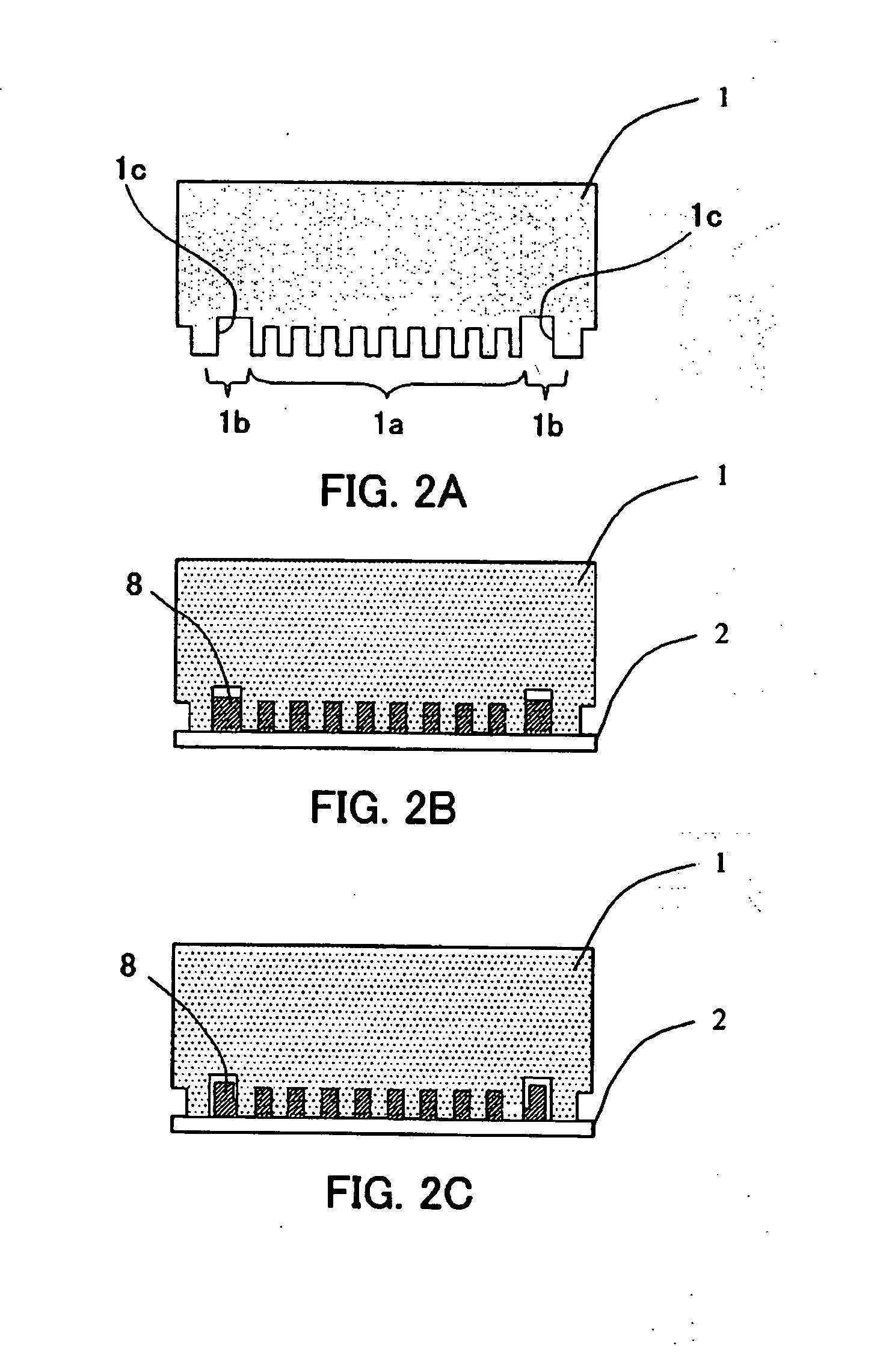
[0066]FIG. 4A shows a pattern transferring mold that is; Embodiment 2 of the present invention in schematic form. The shape of a pattern formed in a patterned area on the mold of this embodiment is the same as that of Embodiment 1. The mold of this embodiment is used in the nanoimprint apparatus described in Embodiment 1.

[0067]101 denotes the mold of this embodiment. 101a denotes a patterned area (first area) where a relief pattern is formed, the patterned area being formed on the bottom face of the mold 101. 101c denotes a non-patterned area (second area) which faces the scribe line on the resist 8.

[0068] In FIG. 4A, 101d denotes a protruded portion which is formed in at least a part of the non-patterned area 101c. The protruded portion 101d is a portion having a mold-releasing shape. The protruded portion 101d has a shape such as a conical shape or a triangular prism shape (wedge shape), in which its sectional area becomes smaller towards its lower end. The height of the protrud...

embodiment 3

[0073]FIG. 5A shows a pattern transferring mold that is Embodiment 3 of the present invention in schematic form. The shape of a pattern formed in a patterned area on the mold of this embodiment is the same as that of Embodiment 1. The mold of this embodiment is also used in the nanoimprint apparatus described in Embodiment 1.

[0074]201 denotes the mold of this embodiment. 201a denotes a patterned area (first area) where a relief pattern is formed, the patterned area being formed on the bottom face of the mold 201. 201c denotes a non-patterned area (second area) which faces the scribe line on the resist 8.

[0075] In FIG. 5A, 201e denotes a through-hole which penetrates the inside of the mold 201 and opens on the non-patterned area and the side face of the mold 201. The shape of the opening 201f of the through-hole 201e on the non-patterned area is a mold-releasing shape. The other opening of the through-hole 201e may be formed on any face of the mold 201 other than the bottom face.

[...


PUM

PropertyMeasurementUnit
Sizeaaaaaaaaaa
Shapeaaaaaaaaaa
Areaaaaaaaaaaa

Abstract

One object of the present invention is to provide a pattern transferring mold which can provide a starting area of mold release easily and certainly and a pattern transferring apparatus with the same. A pattern transferring mold is disclosed which is used in a pattern transferring apparatus that brings the mold into contact with a photo-curing resin on a substrate and cures the photo-curing resin by light irradiation to transfer a pattern formed on the mold onto the photo-curing resin. The mold comprises a bottom face which contacts the photo-curing resin, the bottom face portion including a first area in which the pattern is formed and a second area formed outside the first area. The mold has a mold-releasing shape in the second area, the mold-releasing shape providing a starting area of mold release from the cured photo-curing resin.

Description

BACKGROUND OF THE INVENTION [0001] The present invention relates to a pattern transferring apparatus for manufacturing semiconductor devices or devices having a fine pattern such as MEMS (Micro Electro-Mechanical Systems) and, more specifically, to so-called photo-curing type nanoimprint lithography. [0002] In a photo-curing type nanoimprint apparatus used for nanoimprint lithography, which has been disclosed in U.S. Pat. No. 6,334,960, a liquid ultraviolet (UV) curable resin as a resist is disposed between a substrate and a mold (original plate or template) having a relief pattern, and then the resist is cured by UV irradiation through the mold. The mold is released from the substrate after curing the resist, and the pattern-transferred resist thereby remains on the substrate. [0003] Then, residual layer (base layer) of the resist are removed by executing RIE (reactive ion etching) on the pattern-transferred substrate. Thereby, a pattern is formed on the substrate. [0004] Manufactu...

Claims


Application Information

Patent Timeline
IPC IPC(8): B29C59/02B81C99/00
CPCB81C99/009B81C2201/0152B81C2201/036B82Y10/00B82Y40/00G03F7/0002
Inventor TOKITA, TOSHINOBUOTA, HIROHISAKAWAKAMI, EIGOKASUMI, KAZUYUKINAKAMURA, TAKASHI
Owner CANON KK
Why Eureka
Try Eureka