
Non-volatile semiconductor memory device and data programming method

a technology of non-volatile semiconductors and memory cells, which is applied in the direction of static storage, digital storage, instruments, etc., can solve the problems of dispersion of the electric injection rate of the floating gate of the memory cell, and achieve the effect of improving the data read speed

Inactive Publication Date: 2006-08-31
KK TOSHIBA
View PDF25 Cites 5 Cited by
  • Summary
  • Abstract
  • Description
  • Claims
  • Application Information

AI Technical Summary

Benefits of technology

[0018] With the above described situation in mind, therefore, it is an object of the first aspect of the present invention to provide a non-volatile semiconductor memory device in which large current can be flowed through the memory block to improve the data read speed.

Problems solved by technology

Furthermore, as already described, in the conventional semiconductor memory device, since one column line is formed in correspondence to the memory block of one column, there exist various problems.
Further, in the conventional non-volatile semiconductor memory cell already described on the basis of FIGS. 28 and 29, there exists a drawback in that the electron injection rate to the floating gate of the memory cell disperses due to the dispersion in thickness of the gate insulation film of the memory cell and crystal defects caused by the dispersion during the manufacturing process.

Method used


Image

  • Non-volatile semiconductor memory device and data programming method
  • Non-volatile semiconductor memory device and data programming method
  • Non-volatile semiconductor memory device and data programming method

Examples


Embodiment Construction

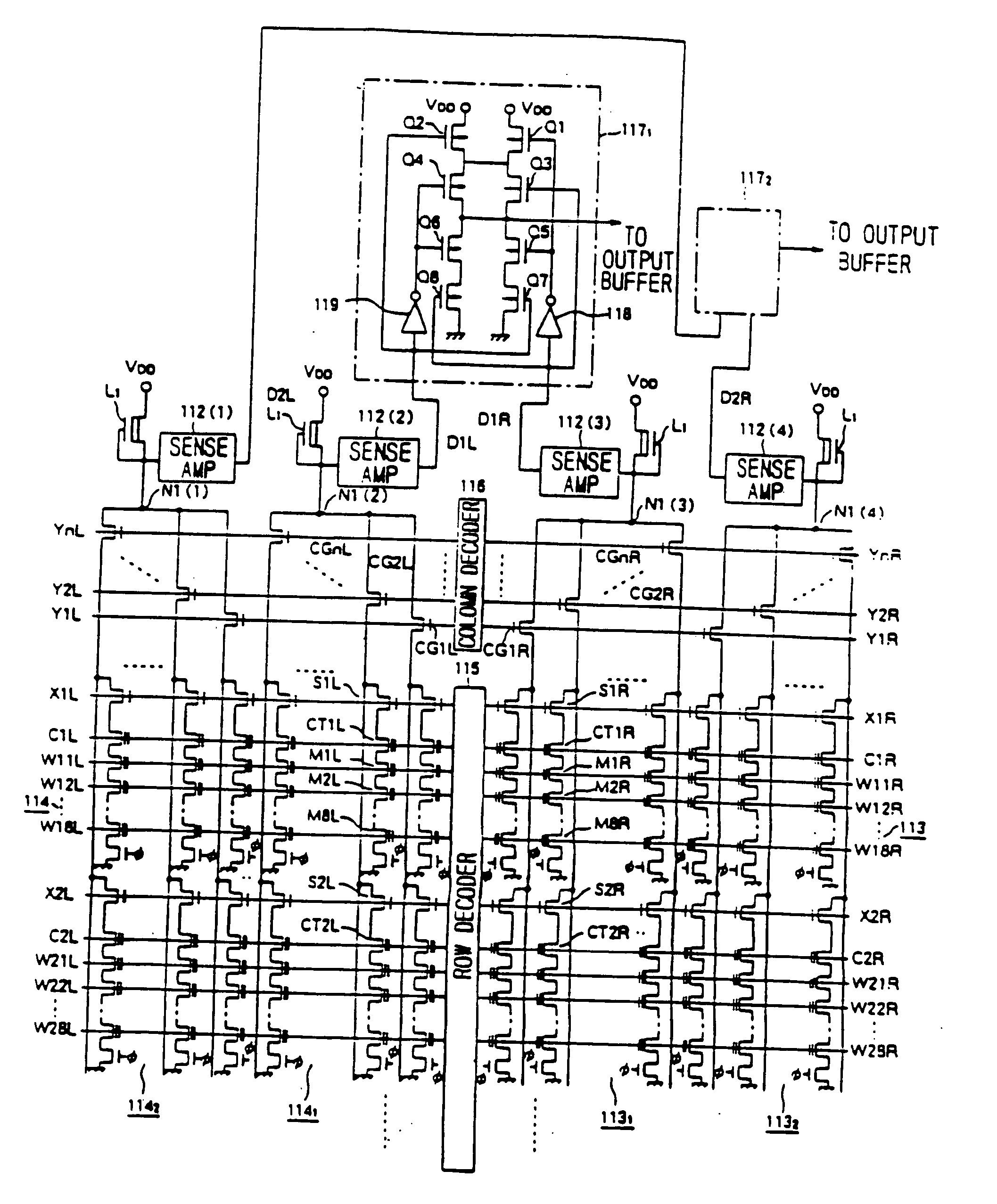
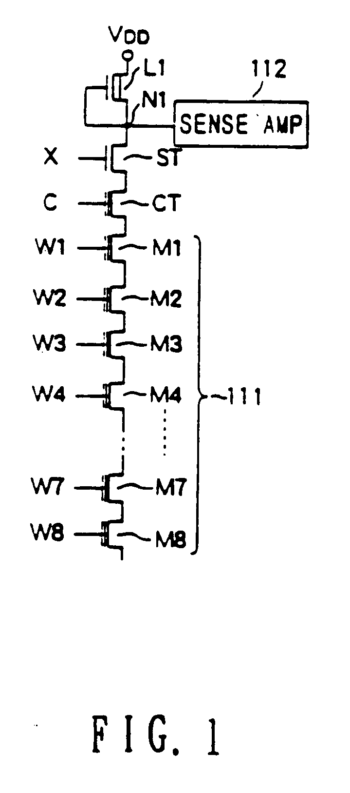
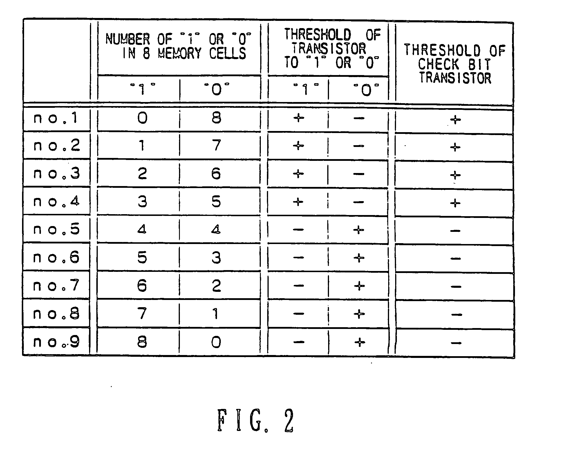
[0081] A first embodiment of the first aspect of the present invention will be described hereinbelow with reference to the drawings. FIG. 1 is a circuit in which a bit checking transistor CT whose conduction state is controlled by signal C is connected between the select transistor ST and the memory cell M1. The bit checking transistor stores whether a memory cell having a negative threshold voltage, which is included the other memory block which is different from the memory block including this bit checking transistor, corresponds to a logic “0” or a logic “1”. In each of the memory blocks, the memory cell having the negative threshold voltage corresponds to a logic “1” and the memory cell having the positive threshold voltage corresponds to a logic “0” if the number of the data of a logic “1” are larger than the number of the data of a logic “0”, on the other hand, the memory cell having the negative threshold voltage corresponds to a logic “0” and the memory cell having the posit...


PUM


Abstract

In a non-volatile semiconductor memory, a large current can be flowed through the memory cell during reading. The number of the column lines can be reduced. The electron injection to the floating gates of the respective memory cells is averaged to reduce the electron emission from the floating gates of the respective memory cells is also averaged to reduce the dispersion of the threshold voltages thereof. An increase in chip size due to latch circuits can be prevented. By noting that either of a plurality of “0” or “1” of the binary data are stored such in the memory cells of the memory cell bundle or block, a negative threshold voltage in allocated to the memory cells for storing the more bit side data of the binary data. A single column line is used in common for the two adjacent memory blocks. To inject electrons to the floating gates of the memory cells, voltage is increased gradually and stopped when electrons have been injected up to a predetermined injection rate. Electrons are once emitted from the floating gates, and thereafter the electrons are injected again to store one of a binary data. Further, the data latch circuits can be formed at any positions remote from the memory cell array.

Description

FIELD OF THE INVENTION [0001] The present invention relates to a non-volatile semiconductor memory device and its data programming method. BACKGROUND OF THE INVENTION [0002] A memory cell of an NAND type EEPROM is shown in FIG. 28. FIG. 28 is a schematic sectional view of the memory cell MC. The gate insulation film GO which is formed between floating gate FG and channel region CA is sufficiently thin to allow an electron tunnel effect to occur between the floating gate FG and the channel region CA. Electrons are emitted from the floating gate FG to the channel region CA by supplying a high voltage to the substrate Sb, and 0V to the control gate CG, so that one of a binary data is stored in the memory cell. On the other hand, when the other of a binary data is stored in the memory cell, electrons are injected from the channel region CA to the floating gate FG. In order to inject electrons to the floating gate FG, a high voltage is supplied to the control gate CG, and 0V is supplied ...

Claims


Application Information

Patent Timeline
Patent Type & Authority Applications(United States)
IPC IPC(8): G11C11/34G11C16/04G11C16/12
CPCG11C16/0483G11C16/12G11C16/24G11C16/26
Inventor IWAHASHI, HIROSHI
Owner KK TOSHIBA
Learn More