
Wiring substrate and manufacturing method thereof

a manufacturing method and wire substrate technology, applied in the field of wire substrates, can solve the problems of increasing the production cost of flexible wire substrates, reducing the reliability of connecting portions, and limiting the method in view of reliability improvement or resistance reduction of connecting portions, etc., to achieve simple and highly reliable connection, improve reliability and characteristics, and reduce production cost

Active Publication Date: 2006-08-31
KIOXIA CORP
View PDF10 Cites 7 Cited by
  • Summary
  • Abstract
  • Description
  • Claims
  • Application Information

AI Technical Summary

Benefits of technology

[0010] An object of the present invention is to provide a wiring substrate with improved reliability and characteristics without losing characteristics such as low cost obtained by printing method by enabling a simple and highly reliable connection between both front and rear faces of the wiring substrate, and a manufacturing method thereof.

Problems solved by technology

These connecting methods have problems that they are forced to have complicated steps to connect both the faces, for example: a foundation layer forming step forming a foundation layer along the internal wall surface of the through hole or via hole by the electroless plating, a resist forming step required before forming the foundation layer, and the like.
However, when the general through-hole connection or the via-hole connection is applied to the connection of both the front and rear faces of the substrate, the production cost of the flexible wiring substrate increases due to the complicated steps and increased number of steps required for the connection as described above.
In other words, the flexible wiring substrate applying the electrophotographic method or the like cannot receive the benefit of low cost due to the step of connecting between both the front and rear faces of the substrate.
However, this method has a limitation in view of reliability improvement or resistance reduction of the connecting portion, and so forth, in that the inside of the through hole is filled based simply on fluidity, viscosity, and the like of the conductive ink.
Due to the deposition method or sputtering applied to the formation of the plating foundation layer, this method cannot avoid a cost increase in connecting both the faces, and in addition to that, the reliability and characteristics of the both-face connecting portion are easily degraded depending on the shape of the pinhole.
Further, as in the conventional through-hole forming steps, a resist-layer forming and removing steps are required, having a problem that the step of connecting both the faces itself becomes complicated.

Method used


Image

  • Wiring substrate and manufacturing method thereof
  • Wiring substrate and manufacturing method thereof
  • Wiring substrate and manufacturing method thereof

Examples


examples 1 to 5

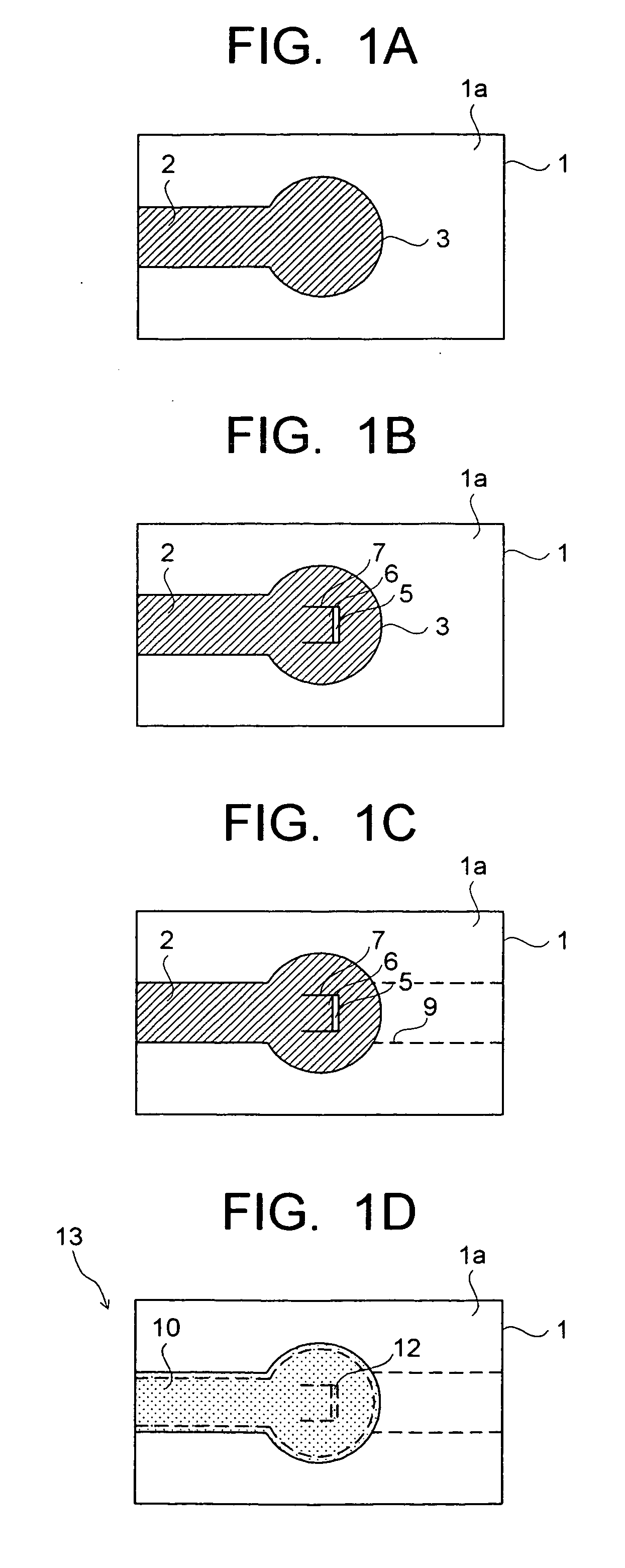
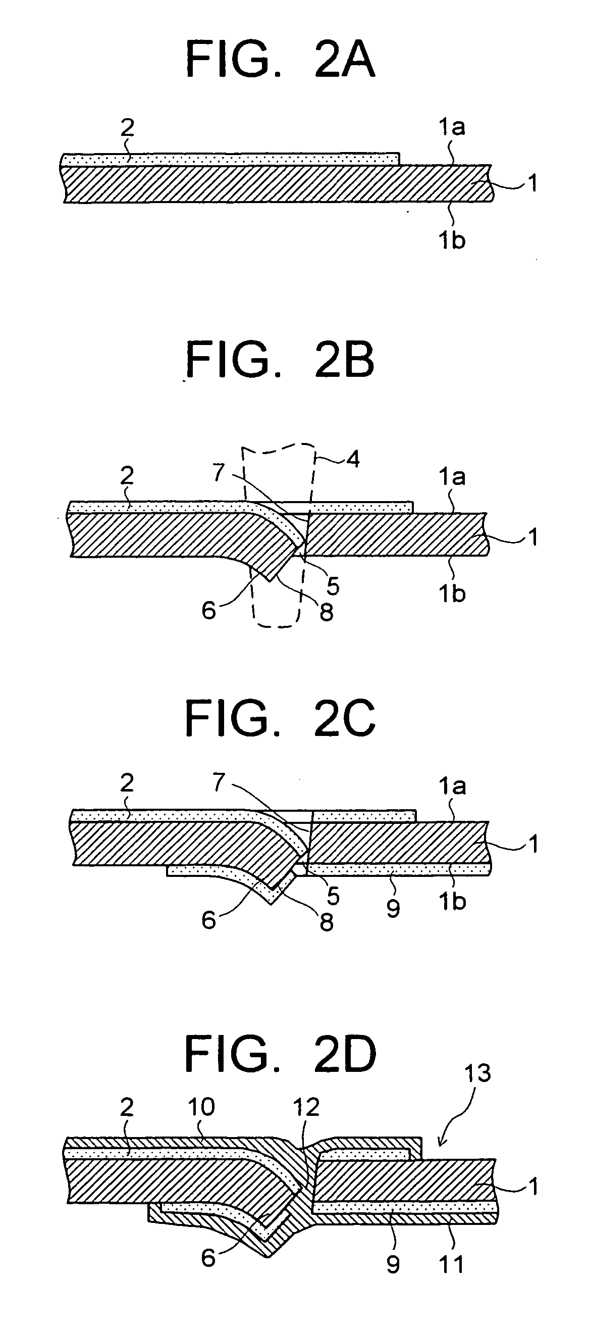
[0056] First, as a toner containing metal particulates and for use in the electrophotographic printing, cresol novolac epoxy resin added and mixed with 50% copper powders by mass, which have a particle diameter of 0.7 μm in average, is prepared. With such toner containing metal particulates, the first plating foundation layer is formed by printing on the front face side of the sheet-shaped insulating substrate. As a sheet-shaped insulating substrate, a glass-epoxy sheet of a thickness of 50 μm (example 1), a polyimide sheet of a thickness of 25 μm (example 2), a polyimide sheet of a thickness of 50 μm (example 3), a polyimide sheet of a thickness of 75 μm (example 4), and a PET sheet of a thickness of 50 μm (example 5) are used. The printings of the toner containing metal particulates are performed by a copying machine for office use with 600 dpi resolution.

[0057] Subsequently, a through hole is formed in each sheet-shaped insulating substrate having the first plating foundation la...

examples 6 to 10

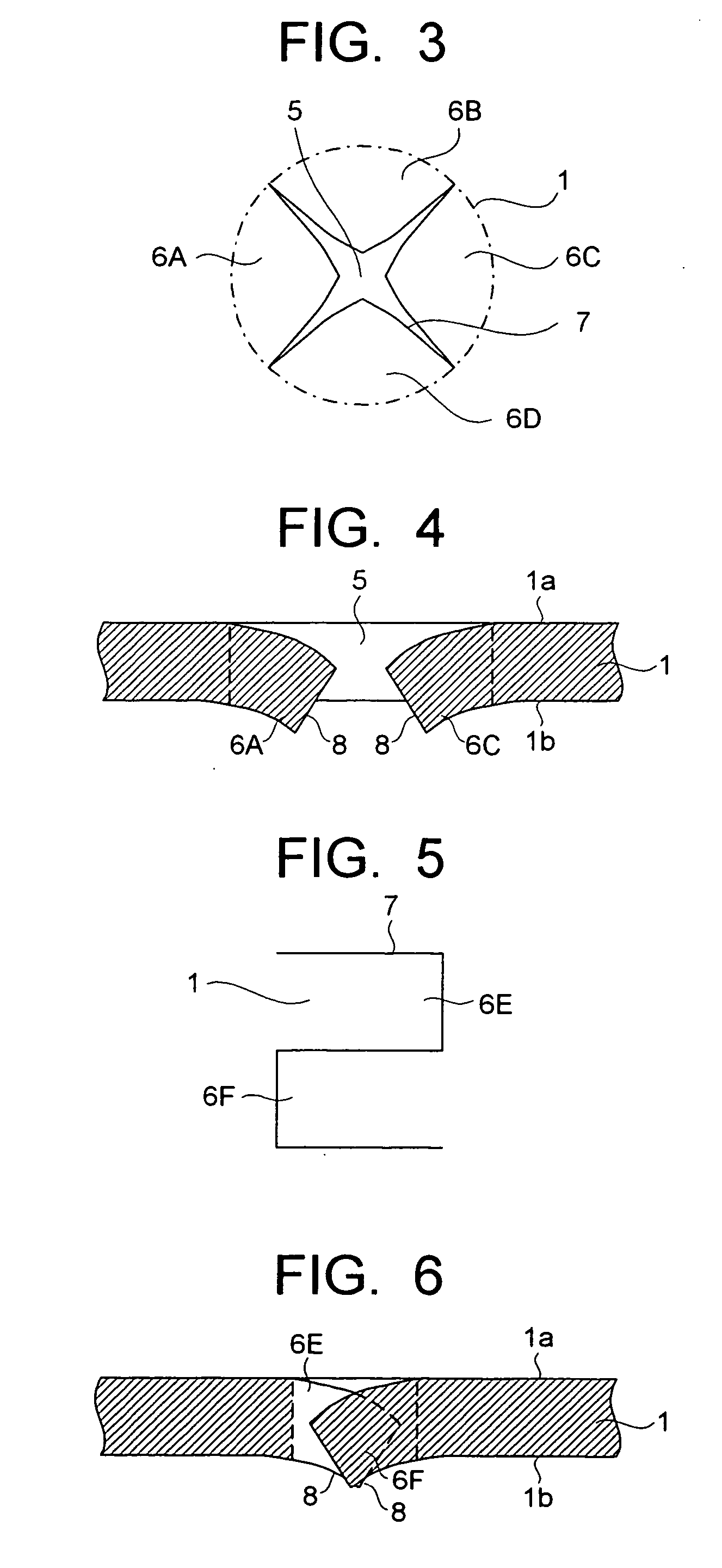
[0060] The through holes are formed with respect to the same sheet-shaped insulating substrate as in Examples 1 to 5 by applying laser machining. At this time, the tapered through holes are formed by controlling laser output. The tilting angle α of the tapered through hole is defined to be within the range from 30 degrees to 80 degrees. Apart therefrom, a totally-tilting through hole is formed by controlling the angle to process by the laser machining. The tilting angle α of the totally-tilting through hole is also defined to be within the range from 30 degrees to 80 degrees. Incidentally, for the respective sheet-shaped insulating substrates, that having the tapered through hole formed and that having the totally-tilting through hole formed are produced.

[0061] On the sheet-shaped insulating substrates having the tilting through holes as described above, the first and second plating foundation layers are formed sequentially by printing using the toner containing the same metal part...


PUM

PropertyMeasurementUnit
thicknessaaaaaaaaaa
tilting angleaaaaaaaaaa
thicknessaaaaaaaaaa

Abstract

A first plating foundation layer is formed by printing on a front face of a sheet-shaped insulating substrate. By inserting a punch into the sheet-shaped insulating substrate having the first plating foundation layer, a through hole is formed while leaving a piece having the plating foundation layer in the portion where the punch is inserted. A second plating foundation layer is formed by printing on a rear face of the sheet-shaped insulating substrate. A first and second wiring layers composed of a metal plating layer are formed by performing electroless plating, and at the same time, a metal plating layer connecting between the first and second wiring layers is formed in the through hole using the plating foundation layer on the piece.

Description

CROSS-REFERENCE TO THE RELATED APPLICATIONS [0001] This application is based upon and claims the benefit of priority from the prior Japanese Patent Applications No. 2005-042170, filed on Feb. 18, 2005; the entire contents of which are incorporated herein by reference. BACKGROUND OF THE INVENTION [0002] 1. Field of the Invention [0003] The present invention relates to a wiring substrate and a manufacturing method thereof. [0004] 2. Description of the Related Art [0005] In recent years, when producing a wiring substrate on which parts such as a semiconductor element, a chip, and so forth are to be mounted, the application of printing methods represented by an electrophotographic method, a screen printing, and the like is under study, and their practical uses are in progress (refer to, for example, Japanese Patent Laid-Open Application No. Hei7-263841 and Japanese Patent Laid-Open Application No. 2004-048030). For instance, a plating foundation layer is formed on an insulating substrat...

Claims


Application Information

Patent Timeline
Patent Type & Authority Applications(United States)
IPC IPC(8): B05D5/12
CPCH05K3/1266Y10T428/24917H05K3/4084H05K3/422H05K2201/09081H05K2201/091H05K2201/09563H05K2201/09827H05K2203/0221H05K2203/0517H05K2203/0709Y10T29/49167Y10T29/49165Y10T29/49124Y10T29/49117Y10T29/49155H05K3/182H05K3/18
Inventor YAMAGUCHI, NAOKOAOKI, HIDEO
Owner KIOXIA CORP
Learn More