Canceling harmonics in semiconductor RF switches

a technology of rf switch and harmonics, applied in the field of semiconductor rf switch cancelling harmonics, can solve the problems of bulk cmos rf switch disadvantageously exhibiting high insertion loss, improving rf switch performance with mixed, and varying degree of integrated circuit complexity and yield

Active Publication Date: 2006-08-31
PSEMI CORP
View PDF18 Cites 101 Cited by
  • Summary
  • Abstract
  • Description
  • Claims
  • Application Information

AI Technical Summary

Benefits of technology

[0014] Methods and circuits are described herein that enable unwanted harmonic content to be canceled from an input signal being conducted by an RF switching circuit, by establishing compensation...

Problems solved by technology

Prior art RF switch implementations have attempted to improve the RF switch performance with mixed results, and with varying degrees of integrated circuit complexity and yield.
For example, bulk CMOS RF switches disadvantageously exhibit high insertion loss, low compression, and poor linearity performance characteristics.
For example, GaAs technology exhibits relatively low yields of properly functioning integrated circuits.
GaAs RF switches tend to be relatively expensive to design and manufacture.
In addition, although GaAs switches exhibit good insertion loss characteristics as described above, they may have low-frequency limitations due to slow states that are present in the GaAs substrate.
The technology also does not lend itself to high levels of integration.
Consequently, complex digital control circuitry associated with GaAs RF switches must be implemented “off chip” from the switch.
Even the low power control circuitry associated with the switch has proven diffic...

Method used


Image

  • Canceling harmonics in semiconductor RF switches
  • Canceling harmonics in semiconductor RF switches
  • Canceling harmonics in semiconductor RF switches

Examples


Embodiment Construction

[0037] Throughout this description, the preferred embodiment and examples shown should be considered as exemplars, rather than as limitations on the present invention.

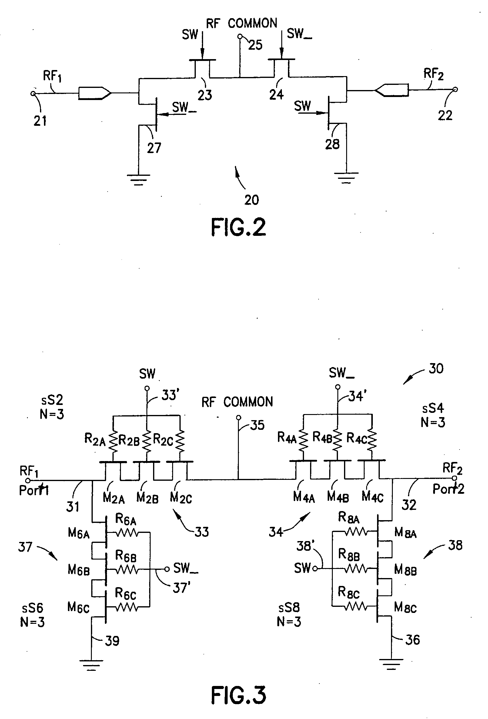
[0038]FIG. 3 represents four semiconductor switching elements that function as an SPDT RF switch 30, similarly as the RF switching circuit described above with reference to FIG. 2. RF switch 30 includes input clamps to prevent signal feedthrough between an unselected input and the conducted signal. Switching elements 33, 34, 37 and 38 are each a FET “stack” that has three insulated gate FETs (such as MOSFETS) coupled in series. The gate of each of the FETs in a stack is coupled to a control voltage (SW or its inverse, SW_) via a gate resistance. If the gate RC product (gate resistance multiplied by the corresponding gate-channel capacitance) of each FET in a stack is substantially the same, and is long compared to the period of the signal being switched, then this arrangement will distribute the voltage applied to the...


PUM


Abstract

An RF switching circuit adapted to cancel selected harmonic signals. An unwanted harmonic signal Sh1 at a selected harmonic frequency Fsh of an operating frequency Fo exists in a signal Si conducted by the switching circuit, possibly produced by the switching circuit due to conduction through a first nonlinear impedance Znl(1). A compensating harmonic signal Sh2 is therefore generated by conduction via a nonlinear impedance Znl(2). Znl(1) may be due to parasitic conduction by “off” switching elements, while Znl(2) may be due to conduction by an “on” FET. The amplitude and/or phasing of Sh2 may be adjusted by selecting components for a network coupling Znl(2) to the conducted signal Si, such that Sh2 substantially cancels Sh1 across a target range of input power.

Description

CROSS REFERENCE TO RELATED APPLICATIONS [0001] This application claims the benefit under 35 USC 119 of U.S. Provisional Application 60 / 650,032, filed Feb. 3, 2005 and entitled “Canceling Harmonics in Semiconductor RF Switches,” and is related to currently pending and commonly owned U.S. patent application Ser. No. 10 / 922,135, filed Aug. 18, 2004 and entitled “Switch Circuit and Method of Switching Radio Frequency Signals,” which in turn claims priority to U.S. patent application Ser. No. 10 / 267,531 (now U.S. Pat. No. 6,804,502), filed Oct. 8, 2002 and entitled “Switch Circuit and Method of Switching Radio Frequency Signals”; and each of these documents is hereby incorporated herein in their entireties by reference.BACKGROUND OF THE INVENTION [0002] 1. Field of the Invention [0003] The present invention relates to semiconductor switching of radio frequency (RF) signals, and in particular to targeted cancellation of harmonics of a fundamental operating frequency (Fo) of an RF signal. ...

Claims


Application Information

Patent Timeline
IPC IPC(8): H04B1/26
CPCH03K17/6871H03K17/693H04B1/48
Inventor KELLY, DYLAN J.
Owner PSEMI CORP
Why Eureka
Try Eureka