Total ionizing dose suppression transistor architecture

Active Publication Date: 2006-09-07
CAES COLORADO SPRINGS LLC
View PDF22 Cites 5 Cited by
  • Summary
  • Abstract
  • Description
  • Claims
  • Application Information

AI Technical Summary

Benefits of technology

[0012] In accordance with an aspect of this invention, a total ionizing dose suppression architecture for a transistor and a transistor circuit uses an “end cap” metal structure that is connected to ground potential voltage to overcome the tendency of negative charge buildup during exposure to ionizing radiation. The suppression architecture of the present invention uses the field established by coupling the metal structure to ground

Problems solved by technology

Such ionizing radiation causes an accumulation of charge in electronic circuits which eventually results in a malfunction or failure of the circuits.
Electron-hole pairs formed near the field oxide of an integrated circuit are more difficult to deal with because the electrons are far more mobile than the holes and may become separated from the holes and trapped near the field oxide interface.
This interferes with recombination and results in an accumula

Method used


Image

  • Total ionizing dose suppression transistor architecture
  • Total ionizing dose suppression transistor architecture
  • Total ionizing dose suppression transistor architecture

Examples


Embodiment Construction

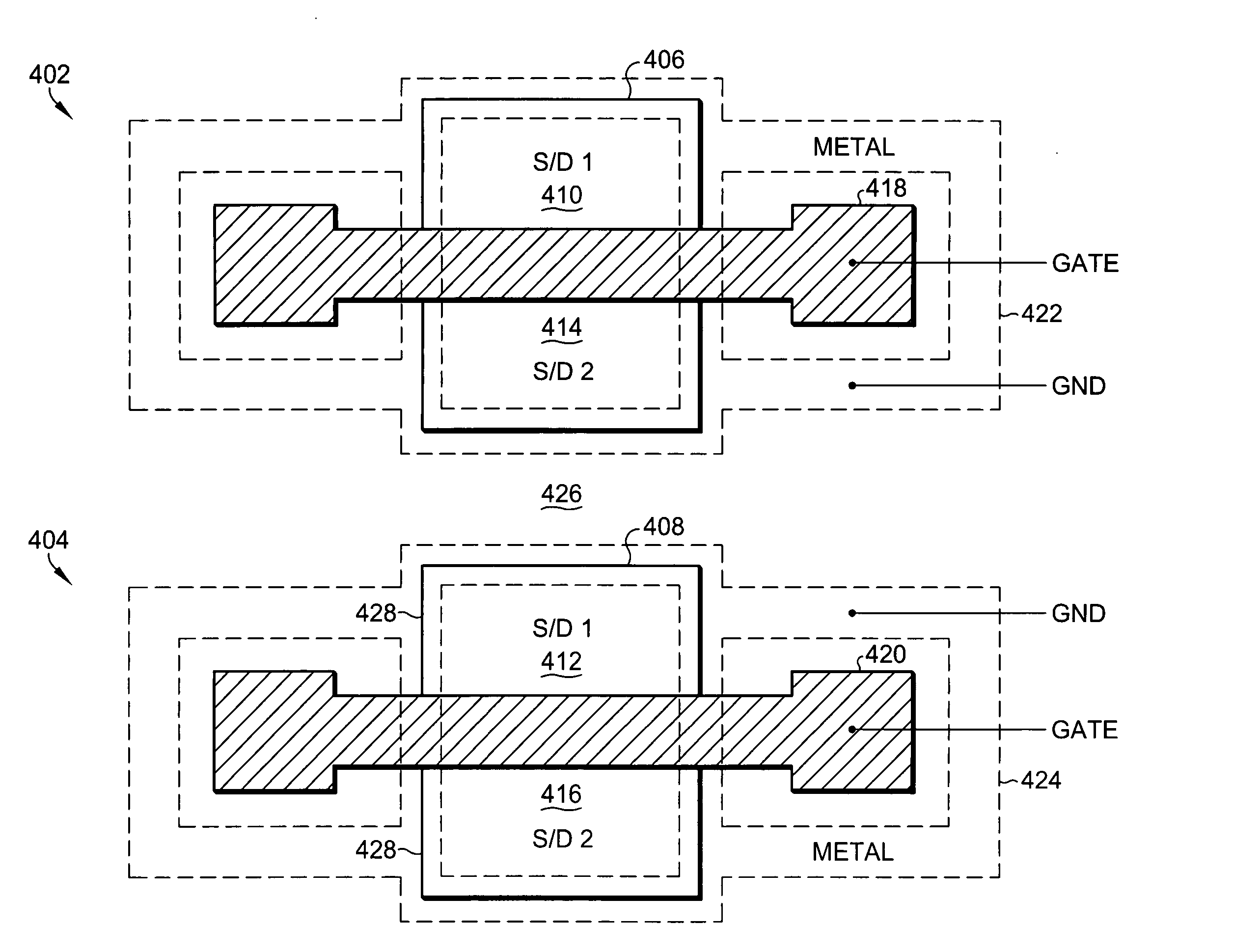
[0033] Referring now to FIG. 4, a plan view of two radiation-hardened N-channel transistors 402 and 404 is shown according to an embodiment of the present invention. A first N-channel radiation-hardened transistor 402 includes an active region 406 surrounded by thick oxide, a polysilicon or metal gate 418 crossing the active region 406, defining first and second source / drain regions 410 and 414. A metal region 422 is coupled to ground and overlaps the boundary of the active region 406, and completely surrounds each of the ends of the gate 418 that extends beyond the border of the active region 406. A second N-channel radiation-hardened transistor 404 includes an active region 408 surrounded by thick oxide, a polysilicon or metal gate 420 crossing the active region 408, defining first and second source / drain regions 412 and 416. A metal region 424 is coupled to ground and overlaps the boundary of the active region 408, and completely surrounds each of the ends of the gate 420 that ex...


PUM


Abstract

A total ionizing dose suppression architecture for a transistor and a transistor circuit uses an “end cap” metal structure that is connected to the lowest potential voltage to overcome the tendency of negative charge buildup during exposure to ionizing radiation. The suppression architecture uses the field established by coupling the metal structure to the lowest potential voltage to steer the charge away from the critical field (inter-device) and keeps non-local charge from migrating to the “birds-beak” region of the transistor, preventing further charge buildup. The “end cap” structure seals off the “birds-beak” region and isolates the critical area. The critical area charge is source starved of an outside charge. Outside charge migrating close to the induced field is repelled away from the critical region. The architecture is further extended to suppress leakage current between adjacent wells biased to differential potentials.

Description

FIELD OF THE INVENTION [0001] The present invention relates to a radiation-hardened transistor architecture and integrated circuit device. BACKGROUND OF THE INVENTION [0002] Electrons trapped in high earth orbits and electrons and protons trapped in low and medium earth orbits cause a high level of ionizing radiation in space. Such ionizing radiation causes an accumulation of charge in electronic circuits which eventually results in a malfunction or failure of the circuits. [0003] Electron-hole pairs generated in the bulk silicon of an integrated circuit do not present a severe problem, as the electrons and holes recombine rapidly. Electron-hole pairs formed near the field oxide of an integrated circuit are more difficult to deal with because the electrons are far more mobile than the holes and may become separated from the holes and trapped near the field oxide interface. This interferes with recombination and results in an accumulation of net positive charge in the field oxide, or...

Claims


Application Information

Patent Timeline
IPC IPC(8): H01L31/00
CPCH01L27/092H01L29/402Y10S257/921Y10S438/953
Inventor GARDNER, HARRY N.
Owner CAES COLORADO SPRINGS LLC
Why Eureka
Try Eureka