

Semiconductor device and method for manufacturing semiconductor device
- Summary
- Abstract
- Description
- Claims
- Application Information
AI Technical Summary
Benefits of technology
Problems solved by technology
Method used
Image

Examples
first embodiment
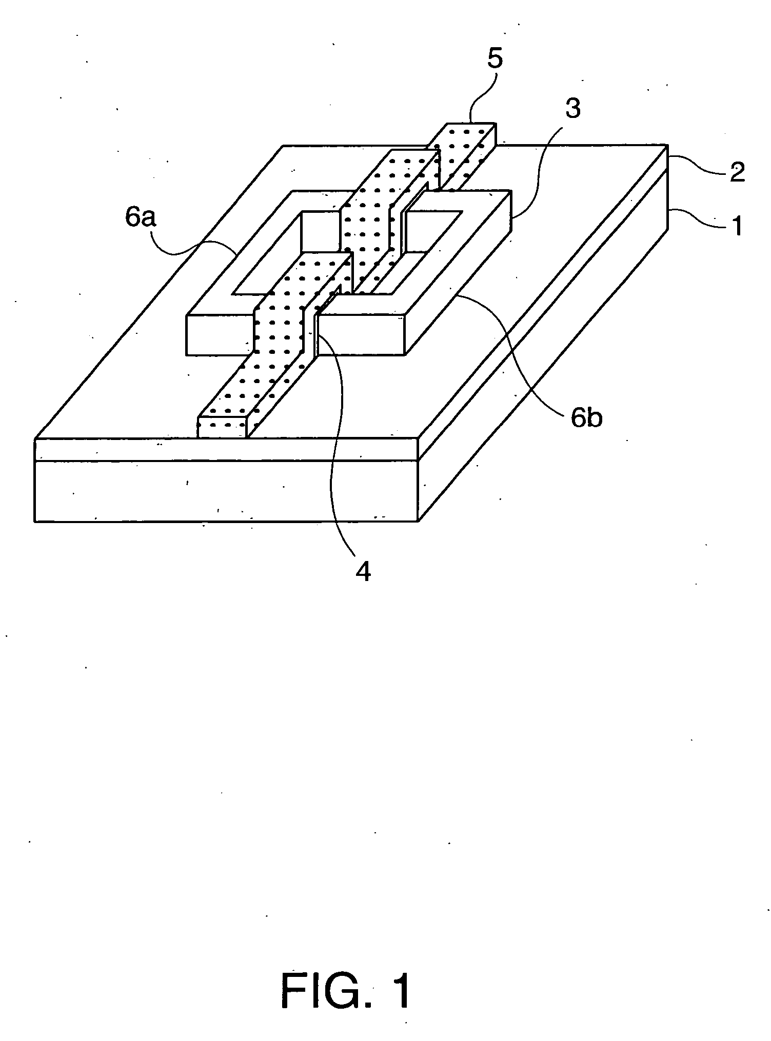
[0065]FIG. 1 is a perspective view showing an outline configuration of a semiconductor device concerning the invention.
[0066] In FIG. 1, an insulating layer 2 is formed on a semiconductor substrate 1, and a semiconductor layer 3 is formed on an insulating layer 2 with epitaxial-growth. Here, the semiconductor layer 3 is epitaxial-grown as to have a film formation face on a side wall, and the semiconductor layer 3 is arranged as to stand steeply on the insulating layer 2. In addition, as the method for arranging the semiconductor layer 3 on the insulating layer 2, the shape of a protrusion, a fin, a box seat, or a mesh may be used, for example. Moreover, the quality of material for the semiconductor substrate 1 and semiconductor layer 3 may be selected from Si, Ge, SiGe, SiGeC, SiC, SiSn, PbS, GaAs, InP, GaP, GaN, or ZnSe, for example. Moreover, for example, FSG (fluoride silicate glass) film or a silicon nitride film, other than a silicon oxide film, may be used. Moreover, as the in...
second embodiment
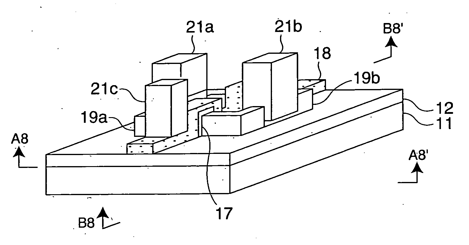
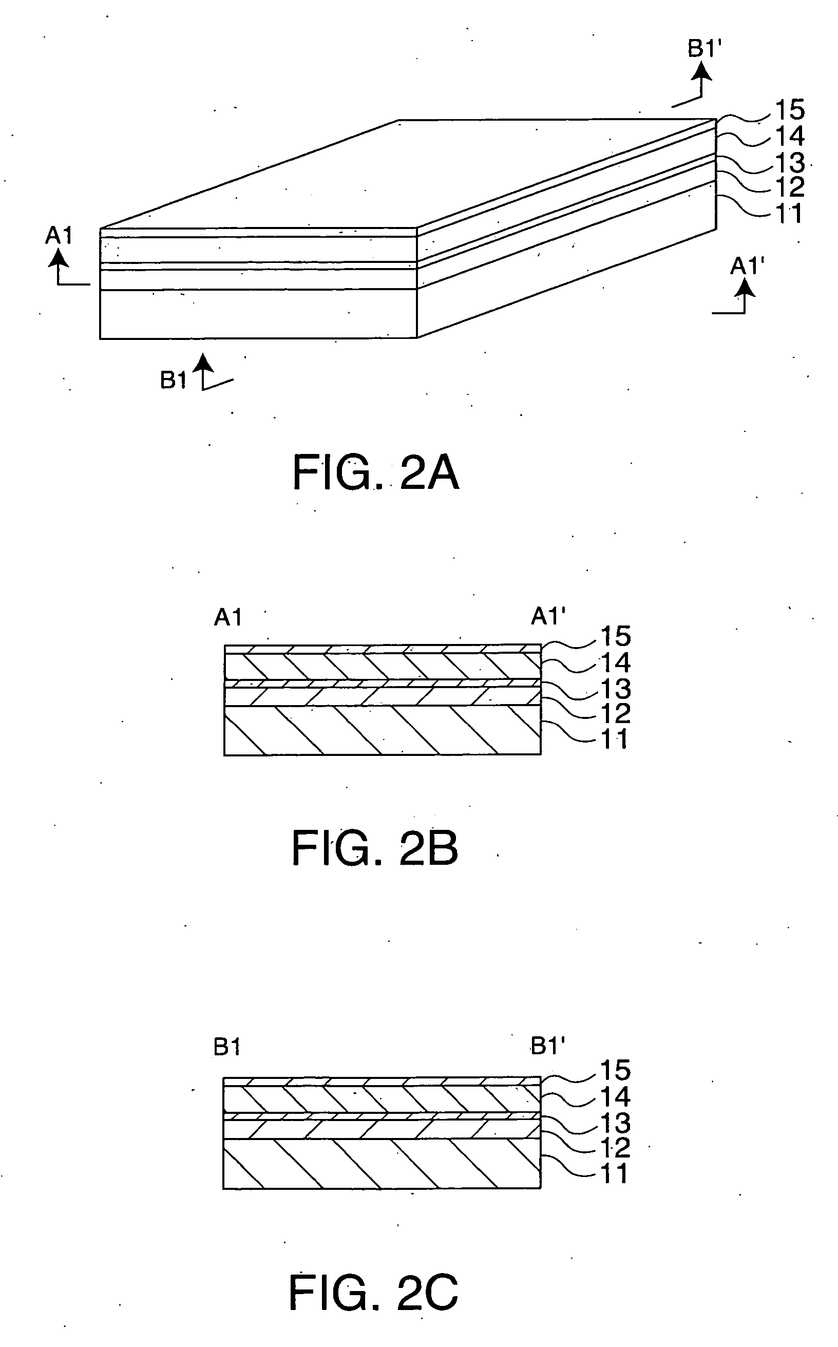
[0070]FIG. 2A through FIG. 9A are perspective views showing the manufacturing method of a semiconductor device concerning the invention, FIG. 2B through FIG. 9B are sectional views cut at A1-A1′ to A8-A8′ lines of FIG. 2A-FIG. 9A, respectively. FIG. 2C through FIG. 9C are sectional views cut at B1-B1′ to B8-B8′ lines of FIG. 2A through FIG. 9A, respectively.
[0071] In FIG. 2, an insulating layer 12 is formed on a semiconductor substrate 11, and a base semiconductor layer 13 is formed on the insulating layer 12. Then, a first semiconductor layer 14 is formed on the base semiconductor layer 13 by carrying out epitaxial-growth. Then, an insulating film 15 is formed on the first semiconductor layer 14 with a method, such as CVD. In addition, as the quality of material of the semiconductor substrate 11, the base semiconductor layer 13, and the first semiconductor layer 14, for example, combinations selected from Si, Ge, SiGe, SiGeC, SiC, SiSn, PbS, GaAs, InP, GaP and GaN, or ZnSe etc. may...
third embodiment
[0087]FIG. 10A through FIG. 21A are perspective views showing the manufacturing method of a semiconductor device concerning the invention, FIG. 10B through FIG. 21B are sectional views cut at A11-A11′ to A21-A21′ lines of FIG. 10A through FIG. 21A, respectively, and FIG. 10C through FIG. 21C are sectional views cut at B11-B11′ to B21-B21′ lines of FIG. 10A through FIG. 21A, respectively.
[0088] In FIG. 10, a first semiconductor layer 32 is film-formed on a semiconductor substrate 31 with epitaxial-growth. Then, an insulating film 34 is formed on the first semiconductor layer 32 with a method such as CVD.
[0089] Next, as shown in FIG. 11, a protrusion 33 that exposes the side wall of the first semiconductor layer 32 is formed in the first semiconductor layer 32 by patterning an insulating film 34 and the first semiconductor layer 32 using a photo lithography technique and etching technique. Here, when forming, on the first semiconductor layer 32, the protrusion 33 that exposes the sid...
PUM
 Abstract
Description
Claims
Application Information