High stress nitride film and method for formation thereof

a nitride film, high stress technology, applied in chemical vapor deposition coatings, electrical devices, coatings, etc., can solve the problems of reducing throughput in comparison to cvd, affecting and causing more complicated geometries. to achieve the effect of increasing the tensile stress of silicon-containing films

Active Publication Date: 2006-09-07
ASM INTERNATIONAL
View PDF99 Cites 486 Cited by
  • Summary
  • Abstract
  • Description
  • Claims
  • Application Information

AI Technical Summary

Benefits of technology

[0017] According to yet another aspect of the invention, a method is provided for semiconductor processing. The method comprises repeatedly separately exposing a substrate to a silane

Problems solved by technology

However, as device density continues to increase and geometries continue to become more complicated, deposition processes have been further refined to meet the need for even more uniform and conformal layers.
While ALD gives superior conformality and uniformity in comparison to CVD, ALD is relatively inefficient in terms of speed.
Consequently, while conformality and uniformity is increased, ALD has the drawback of having decreased throughput in comparison to CVD.
Significant variations in the thickness and/or composition of the silicon-containing compound f

Method used


Image

  • High stress nitride film and method for formation thereof
  • High stress nitride film and method for formation thereof
  • High stress nitride film and method for formation thereof

Examples


example

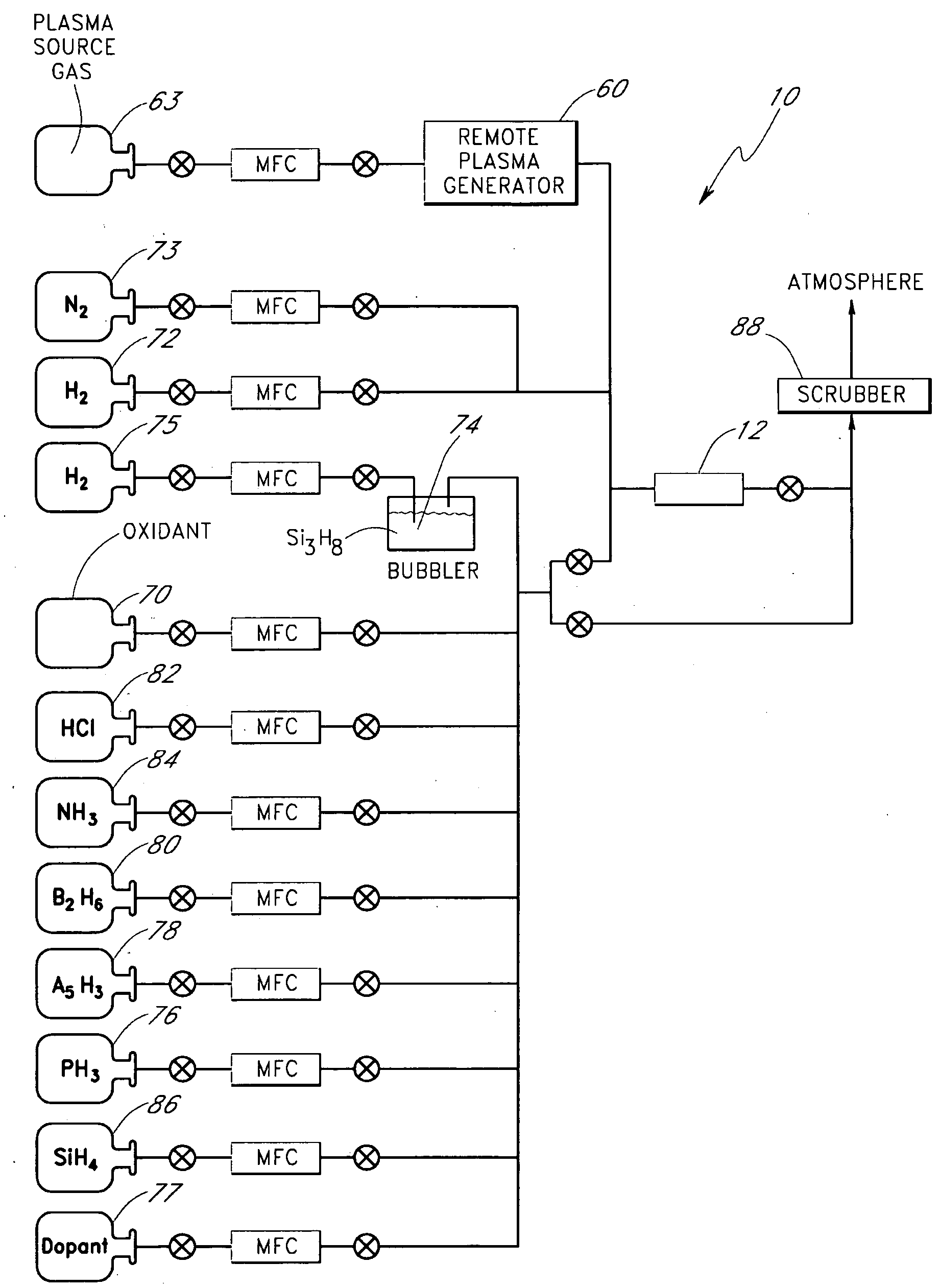
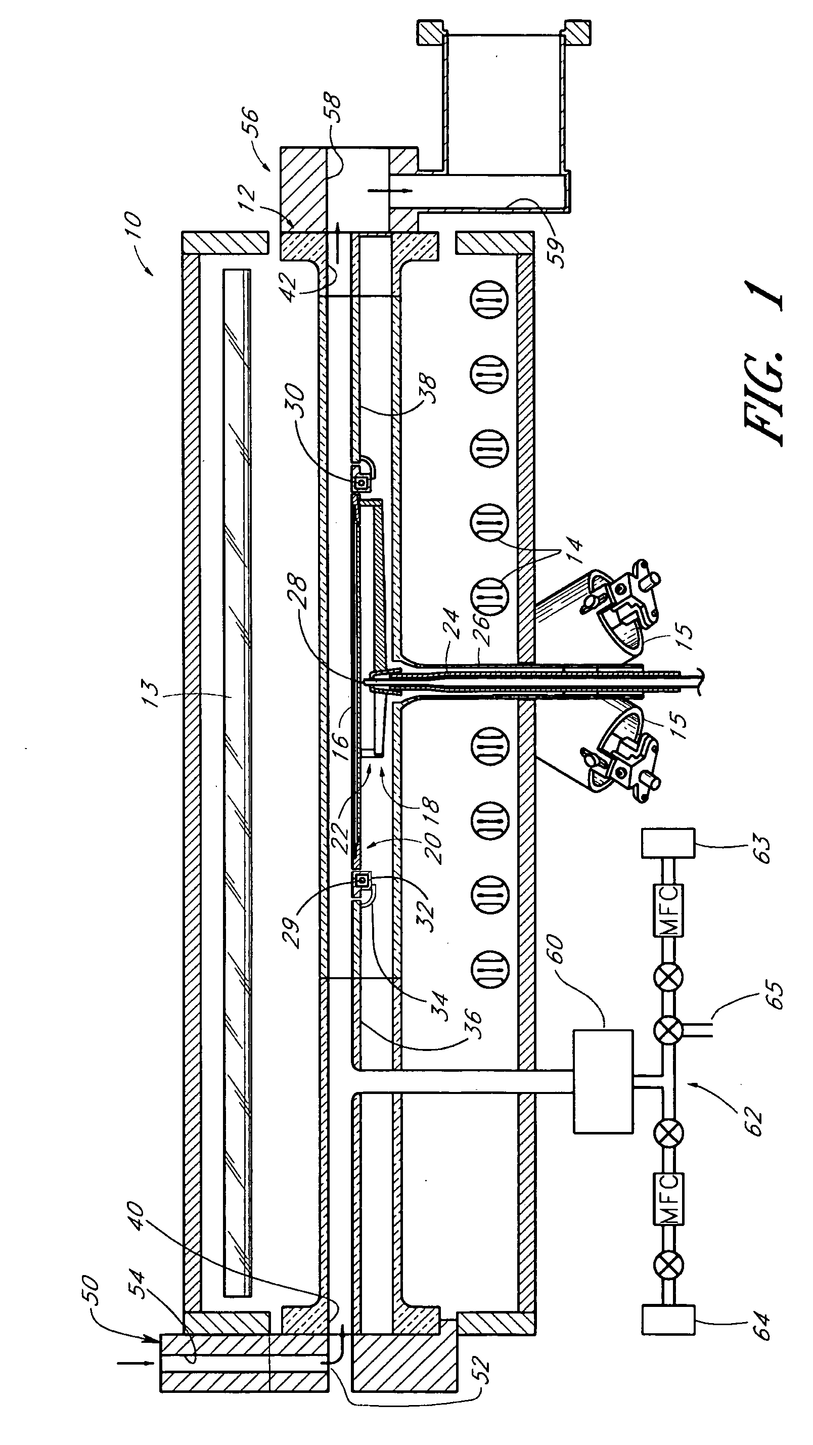
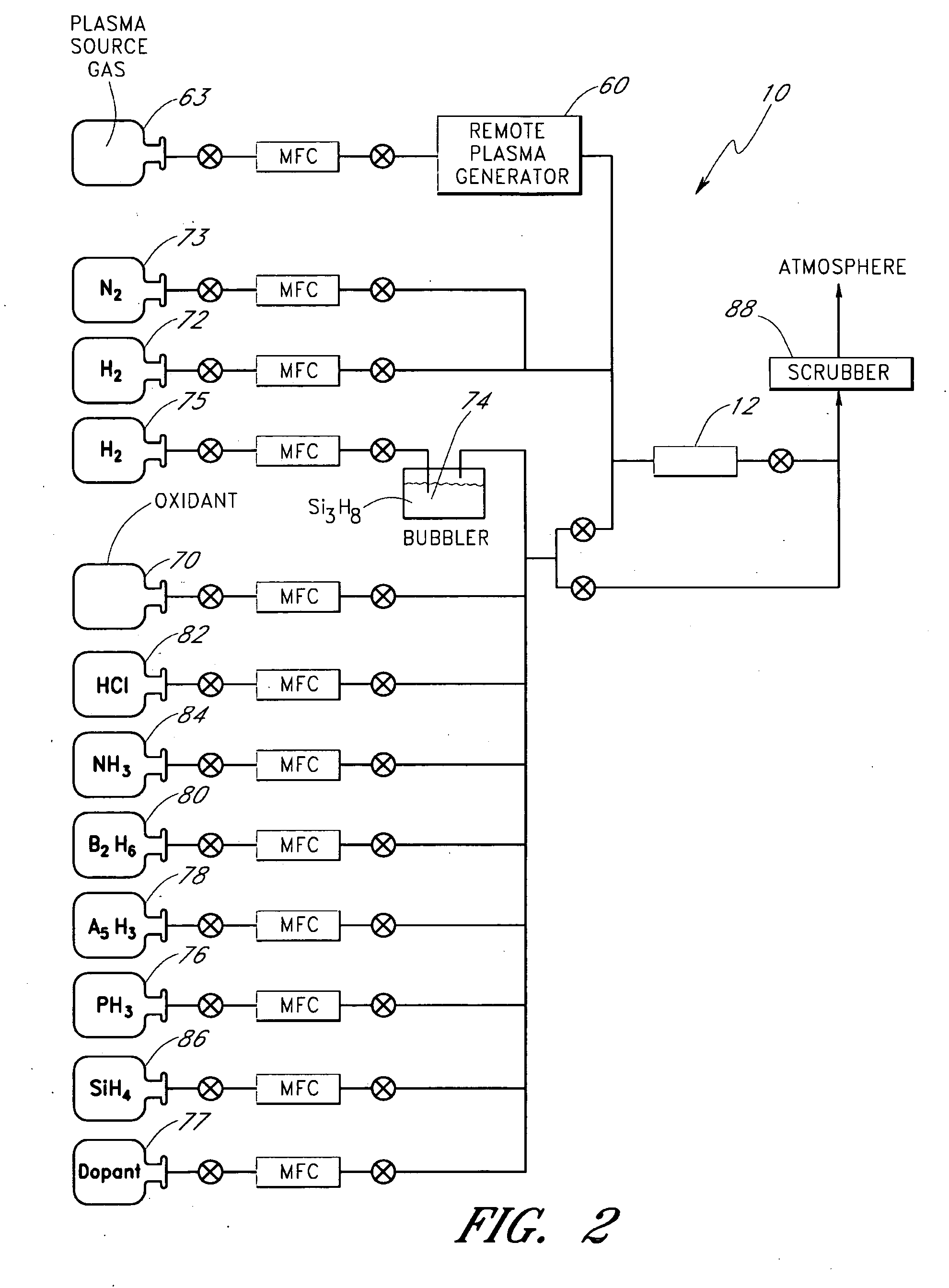
[0144] A carbon doped silicon nitride layer is formed in a batch A412™ reactor from ASM International N.V. of Bilthoven, The Netherlands. For this purpose, a batch of 50 wafers having a diameter of 200 mm is loaded into a wafer boat. The wafer boat is preferably provided with rings which surrounded the edges of the wafers to improve uniformity of the deposited film at those edges. The temperature of the wafers is allowed to stabilize such that the temperature across each wafer is uniform at between about 300° C. and about 500° C., more preferably, each wafer is at a temperature of about 435° C. The boat is preferably rotated about a vertical axis within the reaction chamber. The pressure is preferably set to between about 100 m Torr and about 10 Torr. Trisilane diluted with inert gas is flowed into the reaction chamber at a flow of 20 sccm concurrently with a flow of mono-methyl silane of about 20 sccm, the trisilane partial pressure preferably being 4 mTorr and the exposure time be...


PUM

PropertyMeasurementUnit
Temperatureaaaaaaaaaa

Abstract

A silicon nitride film is formed on a substrate in a reaction chamber by introducing trisilane and a reactive nitrogen species into the chamber in separate pulses. A carbon precursor gas is also flowed into the chamber during introduction of the trisilane and/or during introduction of the reactive nitrogen species, or in pulses separate from the trisilane and reactive nitrogen species pulses. The carbon is used as a dopant in the silicon nitride film and advantageously allows a high stress silicon nitride film to be formed.

Description

REFERENCE TO RELATED APPLICATIONS [0001] This application claims the priority benefit under 35 U.S.C. § 119(e) of U.S. Provisional Application 60 / 659,454, filed Mar. 7, 2005. [0002] In addition, this application is related to: U.S. Patent Application No. 60 / 605,068, STOICHIOMETRIC SILICON COMPOUNDS DEPOSITION IN BATCH FURNACES, filed Aug. 27, 2004; U.S. patent application Ser. No. 10 / 623,482, METHOD TO FORM ULTRA HIGH QUALITY SILICON-CONTAINING LAYERS, filed Jul. 18, 2003, which claims the priority benefit of U.S. Provisional Application No. 60 / 397,576, METHOD TO FORM ULTRA HIGH QUALITY SILICON-CONTAINING LAYERS, filed Jul. 19, 2002; U.S. patent application Ser. No. 10 / 074,564, THIN FILMS AND METHODS OF MAKING THEM, filed Feb. 11, 2002; and U.S. patent application Ser. No. 10 / 074,563, IMPROVED PROCESS FOR DEPOSITION OF SEMICONDUCTOR FILMS, filed Feb. 11, 2002. The disclosure of each of these references is incorporated herein by reference in its entirety.BACKGROUND OF THE INVENTION [...

Claims


Application Information

Patent Timeline
IPC IPC(8): H01L21/00H01L21/31
CPCC23C16/345C23C16/45523H01L21/3115H01L21/3185H01L21/67017H01L21/67115H01L29/7833H01L29/7843H01L21/02205H01L21/02115H01L21/02321H01L21/0217
Inventor WAN, YUET MEIDE BLANK, RENEMAES, JAN WILLEM
Owner ASM INTERNATIONAL
Why Eureka
Try Eureka