Liquid crystal display device and electronic apparatus

Inactive Publication Date: 2006-09-14
SEIKO EPSON CORP
View PDF6 Cites 85 Cited by
  • Summary
  • Abstract
  • Description
  • Claims
  • Application Information

AI Technical Summary

Benefits of technology

[0016] An advantage of the invention is to provide a highly reliable liquid crystal display device with enhanced light utilization efficiency, a wide visible angle, and high visibility, and to provide an electronic apparatus having the liquid crystal display device.
[0017] According to an aspect of the invention, a liquid crystal display device of the present invention is a liquid crystal display device having a first substrate, a second substrate, a liquid crystal layer disposed between the first and second substrates, and a plurality of pixels each having a display region, in that: the liquid crystal layer is optically isotropic when an selective electric field is not applied and optically aisotropic when an electric field is applied and includes a material whose refractive index changes depending on the strength of the electric field; and the plurality of pixels include first and second pixels different in the electric field strength.
[0018] In this case, it is possible to provide the highly reliable liquid crystal display device with enhanced light utilization efficiency, a wide visual angle (wide viewing angle), and high visibility.
[0019] According to another aspect of the invention, a liquid crystal display device

Problems solved by technology

However, by the micro color filter system, it is difficult to satisfactorily increase light utilization efficiency because of color absorption and the like by the color filters.
In a transmission-type liquid crystal display device having a backlight or in a reflection-type liquid crystal display device having a front light, such poor light utilization efficiency becomes the cause for increase in electricity consumption by the

Method used


Image

  • Liquid crystal display device and electronic apparatus
  • Liquid crystal display device and electronic apparatus
  • Liquid crystal display device and electronic apparatus

Examples


first embodiment

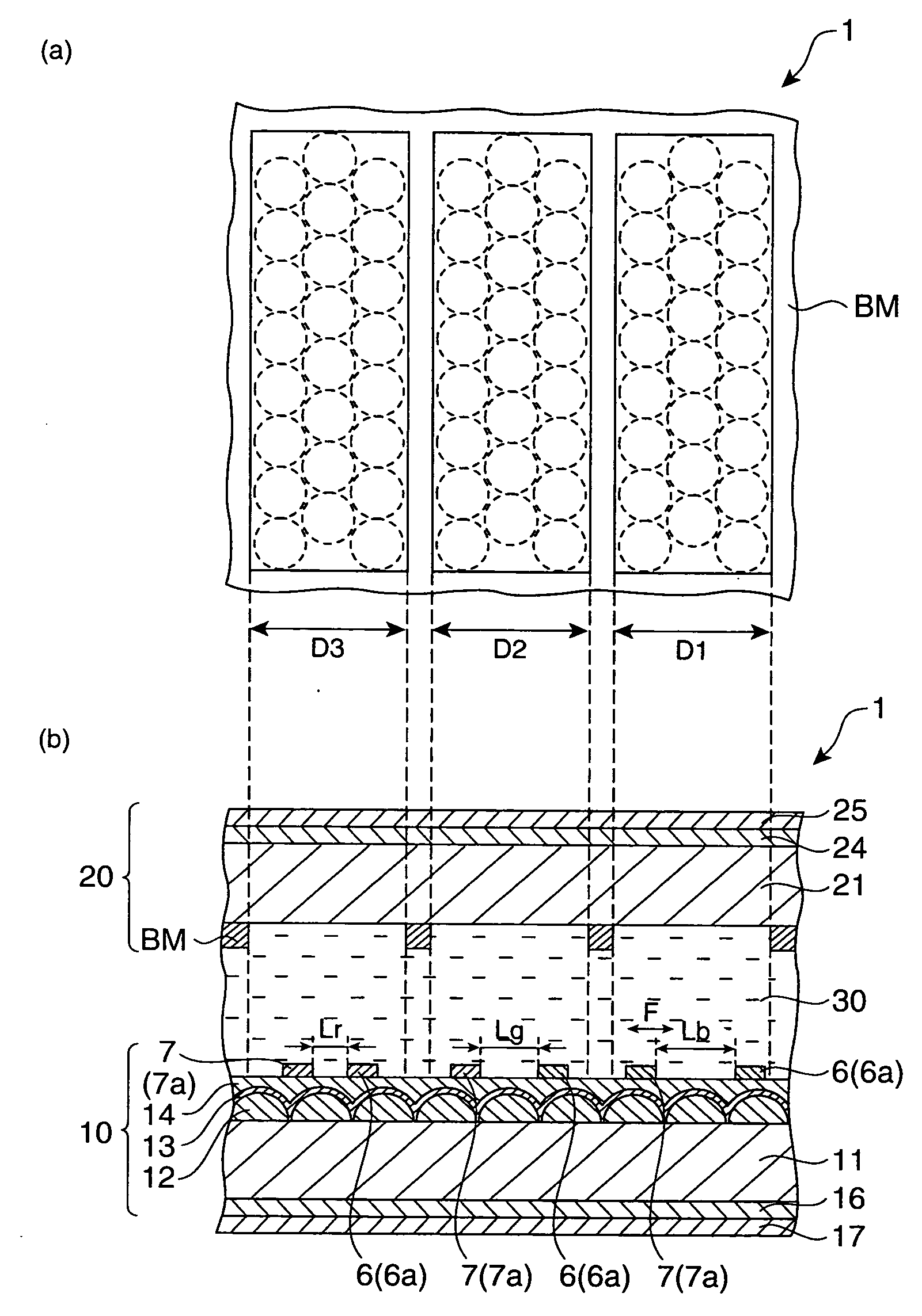
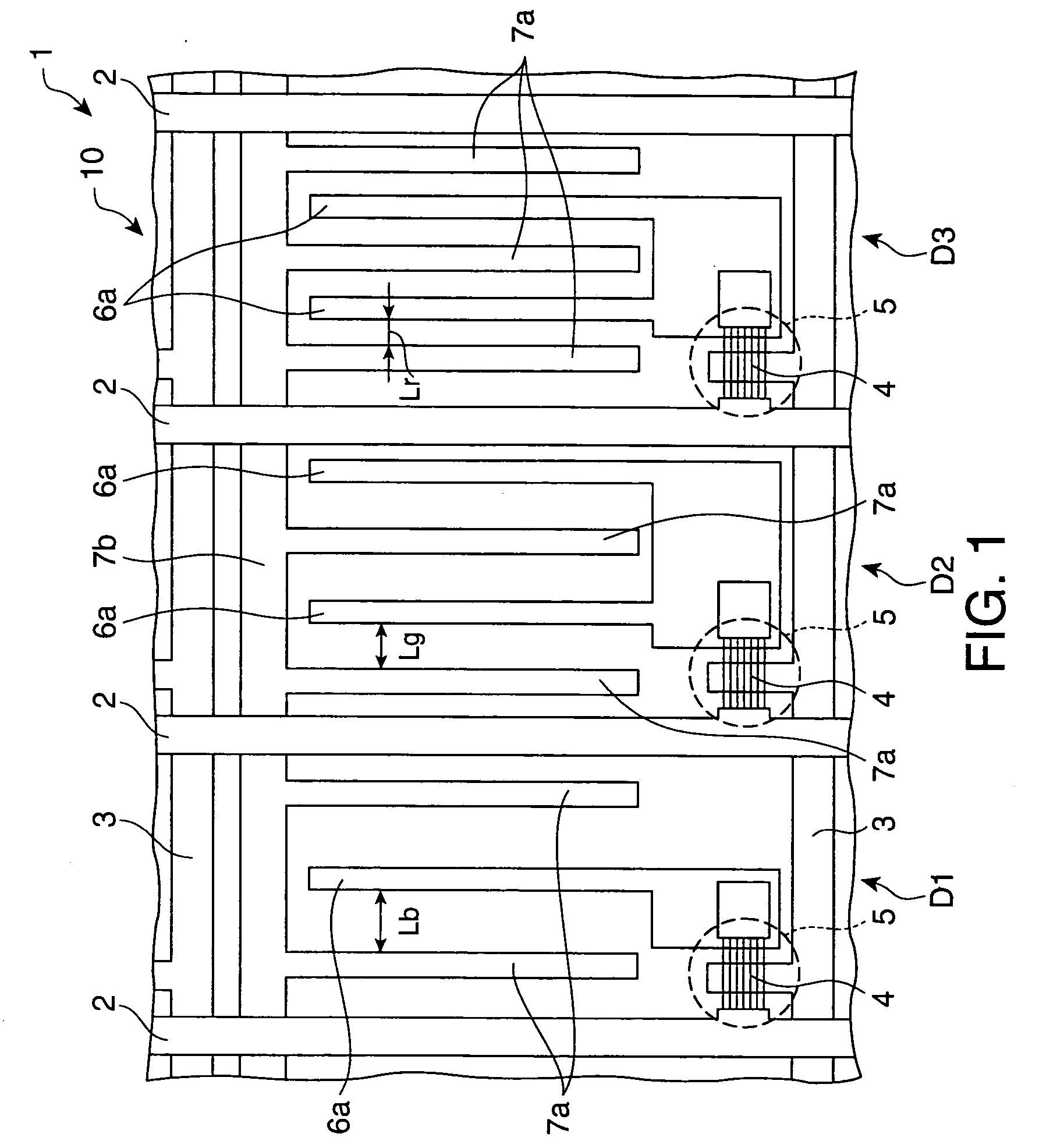
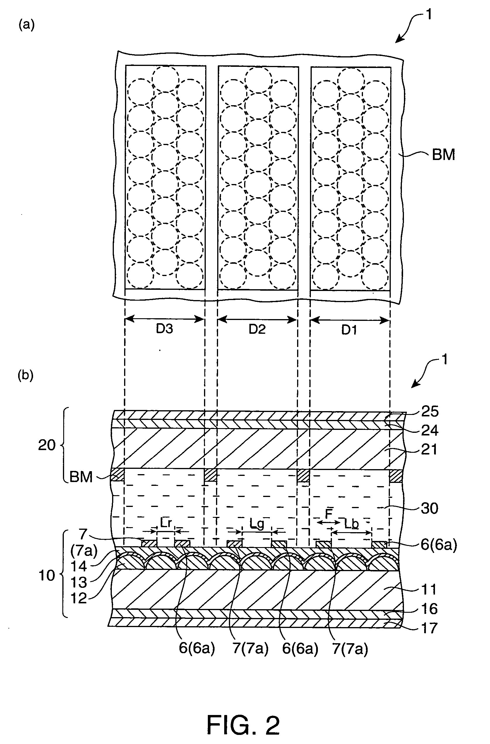
[0055]FIG. 1 is a plan view of an electrode structure of a TFT array substrate of the liquid crystal display device of the first embodiment. FIGS. 2A and 2B are pattern diagrams of the liquid crystal display device of the embodiment, in that FIG. 2A is a plan pattern view to explain three display regions of the liquid crystal display device of the embodiment corresponding to three primary colors, and FIG. 2B is a cross-sectional pattern view of FIG. 2A. Further, for simplicity's sake, FIGS. 1, 2A, and 2B show one enlarged pixel region (one pixel), emphasizing specific portions and altering the ratios of the film thickness, size, and the like of each constituent element where necessary.

[0056] The liquid crystal display device of the embodiment is an exemplary of an active matrix type liquid crystal display device using a thin film transistor (hereinafter referred to as TFT) as the switching element.

[0057] With a liquid crystal display device 1, as shown in FIGS. 2A and 2B, a liquid...

second embodiment

[0115] In the following, the second embodiment of the liquid crystal display device of the invention will be described with reference to the drawings.

[0116]FIGS. 4A and 4B are pattern diagrams showing the liquid crystal display device of the present embodiment. FIG. 4A is a plan pattern diagram to explain the three display regions corresponding to the three primary colors of the liquid crystal display device of the embodiment. FIG. 4B is a cross-sectional pattern view of FIG. 4A. Further, for simplicity's sake, FIGS. 4A and 4B show an enlarged pixel region, emphasizing specific portions and altering the ratios of the film thickness, size, and the like of each constituent element where necessary.

[0117] The liquid crystal display device of the first embodiment is the reflection-type liquid crystal display device (the color liquid crystal display device). In contrast, the liquid crystal display device of the second embodiment is the transmission-type liquid crystal display device (th...

working examples

[0143] Manufacture of Liquid Crystal Material

[0144] As the photopolymerizable monomer, amorphous 2-ethylhexyl acrylate (2EHA) (manufactured by Aldrich Chemical Company), hexyl acrylate (HA) (manufactured by Aldrich Chemical Company), and 1,3,3-trimethylhexyl acrylate (TMHA) (manufactured by Aldrich Chemical Company), and liquid crystalline 6-(4′-cyanobiphenyl-4-yloxy) hexyl acrylate (6CBA) are used. As the crosslinking agent, liquid crystalline diacrylate monomer (RM257) (manufactured by Merck) is used. As the photopolymerization initiator, 2,2-dimethoxy-2-phenylacetophenone (manufactured by Aldrich Chemical Company) is used. As the low molecular liquid crystal material, fluorine-based nematic-mixed liquid crystal, JC-1041XX(7) (manufactured by Chisso Corporation), and cyanobiphenyl-based nematic liquid crystal, 4-cyano-4′-pentylbiphenyl (5CB) (manufactured by Aldrich Chemical Company), are mixed in equal mol. As the chiral dopant, ZLI-4572(9) (manufactured by Merck) is used.

[0145...


PUM

PropertyMeasurementUnit
Coloraaaaaaaaaa
Phaseaaaaaaaaaa
Wavelengthaaaaaaaaaa

Abstract

A liquid crystal display device of the present invention is a liquid crystal display device having a first substrate, a second substrate, a liquid crystal layer disposed between the first and second substrates, and a plurality of pixels each having a display region, in that: the liquid crystal layer is optically isotropic when an selective electric field is not applied and optically aisotropic when an electric field is applied and includes a material whose refractive index changes depending on the strength of the electric field; and the plurality of pixels include first and second pixels different in the electric field strength.

Description

BACKGROUND [0001] 1. Technical Field [0002] The present invention relates to a liquid crystal display device and an electronic apparatus. [0003] 2. Related Art [0004] Flat panel display devices are now used widely in various types of monitors such as for computers as well as in display elements such as for cellular phones. It is predicted that the use of the flat panel display devices will continue to spread more widely, as they are being developed for use in wide-screen TVs. Of all the flat panel displays, the most widely used is a liquid crystal display, which often employs a color display system called a micro color filter system. [0005] The micro color filter system is a system that can easily exhibit high reproduction performance, in that full color display is performed by dividing one pixel into at least three sub-pixels and by forming, in each sub-pixel, color filters of three primary colors of red (R), green (G), and blue (B). However, by the micro color filter system, it is...

Claims


Application Information

Patent Timeline
IPC IPC(8): G02F1/1343
CPCG02F1/133553G02F1/134363G02F1/13731G02F1/1393G02F2001/133541G02F2001/13775G02F1/133541G02F1/13775G02F1/1335
Inventor OZAWA, KINYASHIMAMURA, HIDEO
Owner SEIKO EPSON CORP
Why Eureka
Try Eureka