Plasma display panel

a technology of display panel and plasma, which is applied in the direction of cleaning equipment, address electrodes, carpet cleaners, etc., can solve the problems of pdp needing a large electric power consumption, weak discharge and eventually disappearance, and low discharge efficiency, so as to reduce the generation of electromagnetic interference, shorten the path of electric field, and reduce the effect of pdp

Inactive Publication Date: 2006-09-21
SAMSUNG SDI CO LTD
View PDF14 Cites 2 Cited by
  • Summary
  • Abstract
  • Description
  • Claims
  • Application Information

AI Technical Summary

Benefits of technology

[0022] As described above, the plasma display panel of the present invention includes the first and the second igniting electrodes formed between the first and the second display electrodes and separated dielectric layers independently so as to have each opening formed respectively between the first and the second display electrodes. This arrangement shortens the path of the electric field between the electrodes and achieves low electric power consumption and low generation of electromagnetic interference by improving the discharge efficiency.
[0023] Also, the luminous efficiency of the plasma display panel may be improved by the openings that increase the visible light transmittance to the front substrate.

Problems solved by technology

Therefore, the net voltage difference across the gap between the scan electrode and the address electrode becomes smaller than the initial address voltage (Va), and that causes the discharge to be weak and disappear eventually.
While the dielectric layer with a uniform thickness facilitates the manufacturing process, it lowers a discharge efficiency due to a long path in the electric field where the surface discharge occurs between the sustain electrode and the scan electrode.
As a result, the PDP need a large electric power consumption and emits electromagnetic interference resulted from the high voltage driving.
Also, the uniform thickness of the dielectric layer formed between the sustain electrode and the scan electrode reduces the transmittance of the generated visible light through the front substrate and results in a PDP with low luminance and low luminous efficiency.

Method used


Image

  • Plasma display panel
  • Plasma display panel
  • Plasma display panel

Examples


Embodiment Construction

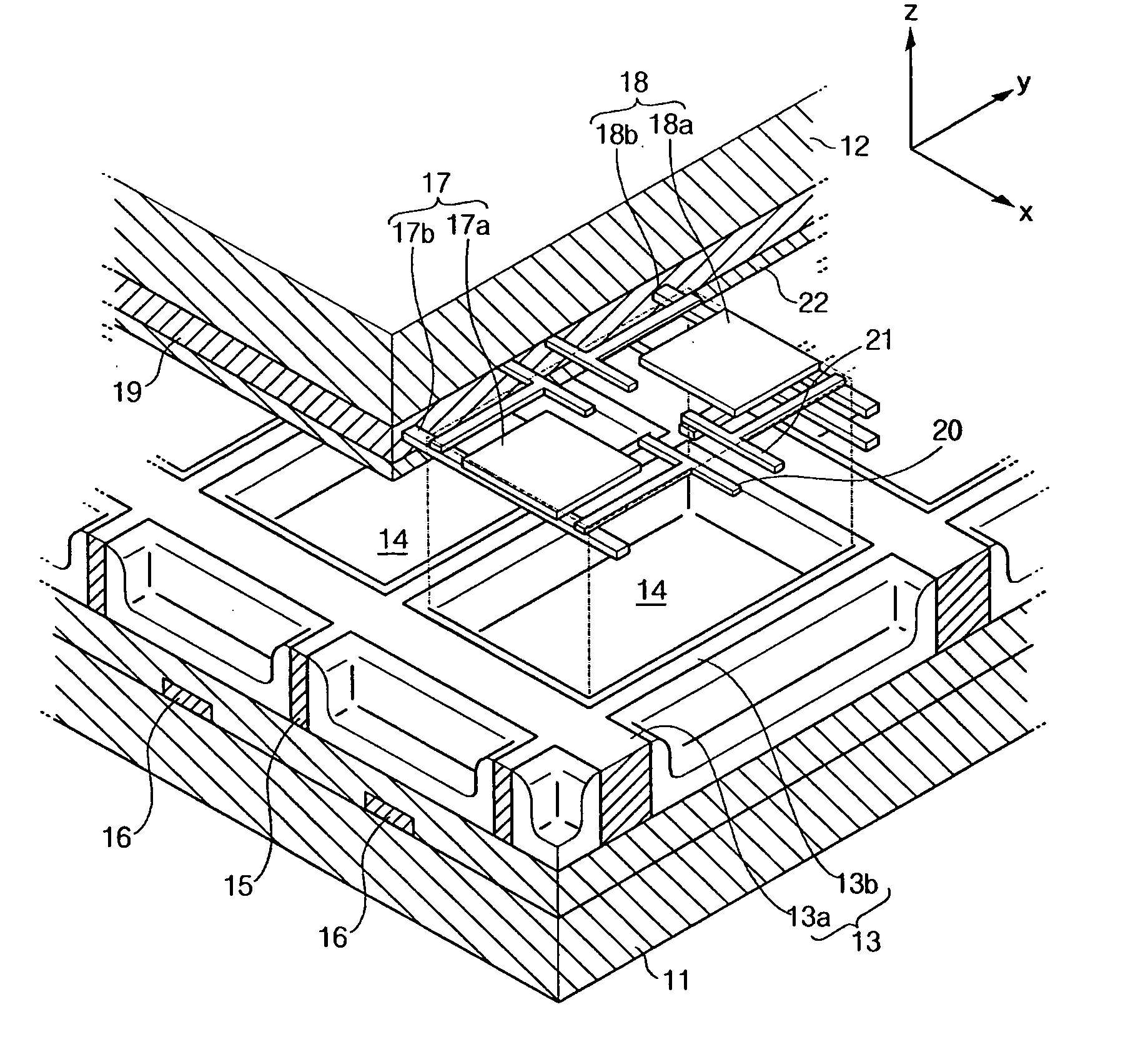
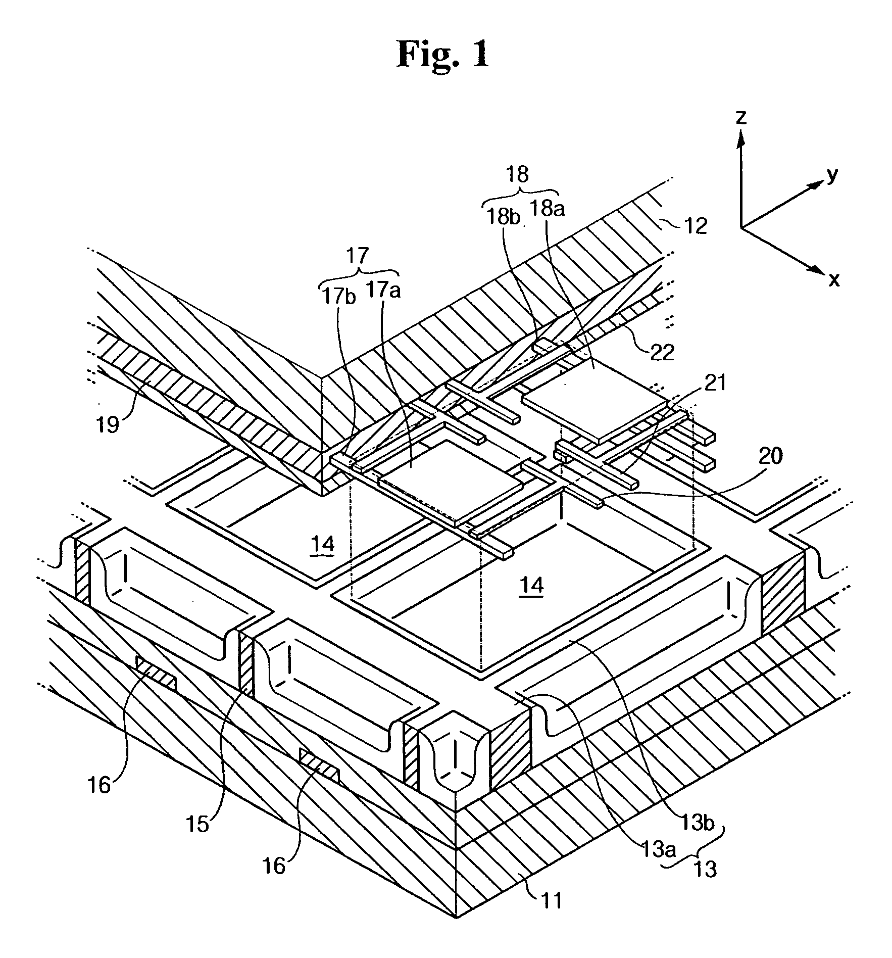
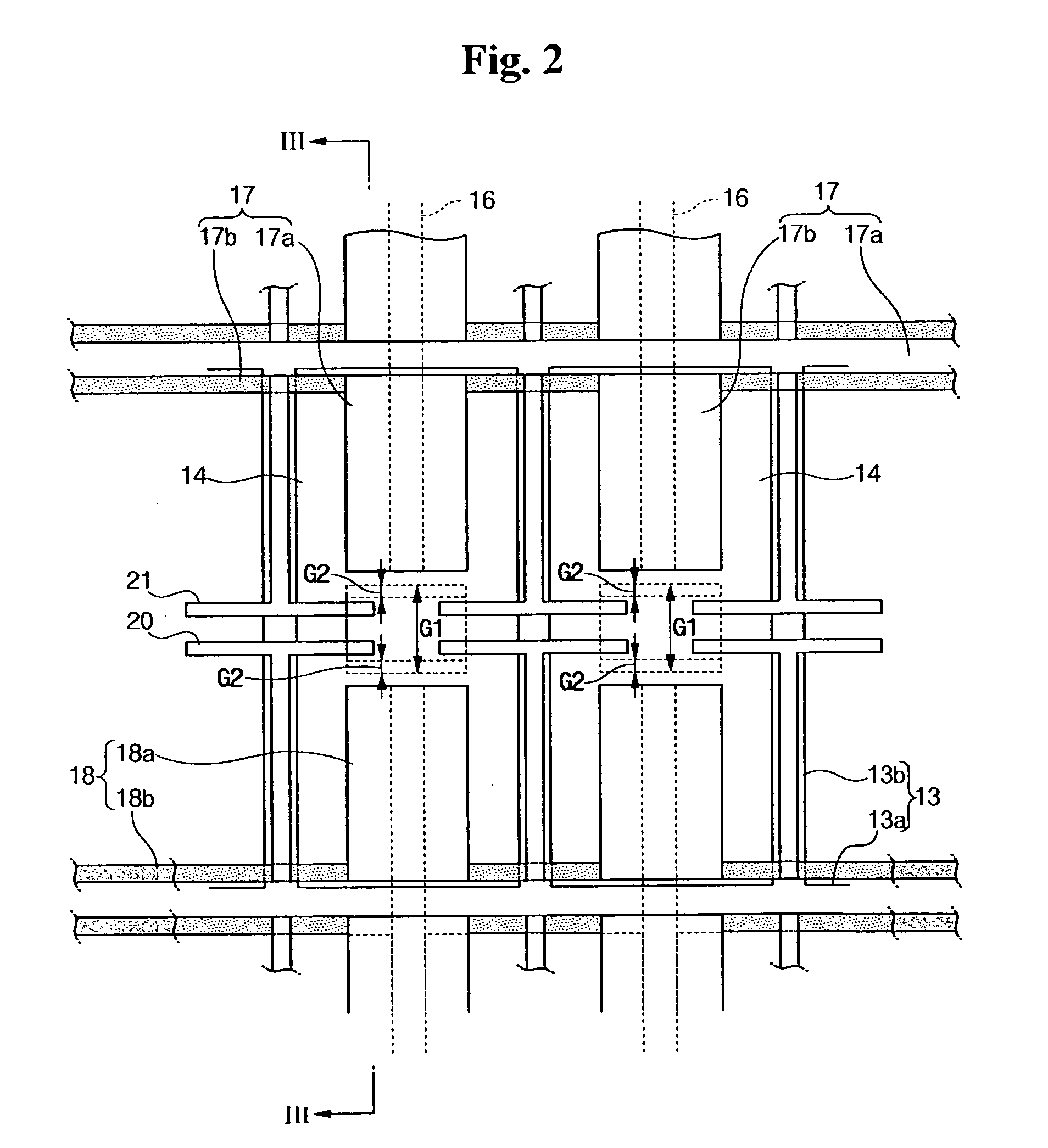
[0030] As shown in FIG. 1, a plasma display panel (PDP) includes a first substrate 11 (a rear substrate); and a second substrate 12 (a front substrate) facing the first substrate 11. A plurality of discharge cells 14 for plasma discharge are formed by a plurality of barrier ribs 13 positioned between the rear substrate 11 and the front substrate 12. A phosphor layer 15 with one of Red (R), green (G) and blue (G) phosphors is formed on the inside of each discharge cell 14.

[0031] On a surface of the rear substrate 11 facing the front substrate 12, formed along a first direction (y-direction) are address electrodes 16 that are positioned in parallel to neighboring address electrodes 16 with a predetermined gap.

[0032] Corresponding to the discharge cells 14, display electrodes, i.e. a first and a second display electrodes 17, 18 are formed on the front substrate 12, extending in a second direction (x-direction) and placed parallel to each other with a pitch of the discharge cells 14 i...


PUM


Abstract

A plasma display panel includes a first substrate and a second substrate facing each other; barrier ribs forming discharge cells between the first substrate and the second substrate; a phosphor layer formed on the inside of the discharge cell; address electrodes formed on the first substrate in a first direction; a first display electrode and a second display electrode, both formed on the second substrate in a second direction crossing the first direction, the display electrodes having at least a pair of enlarged electrodes corresponding to each discharge cell; a first igniting electrode and a second igniting electrode, each formed protruding toward the center of the discharge cell at one end of the extended electrode, over the barrier ribs and along the barrier ribs, respectively from the first display electrode and the second display electrode; a first dielectric layer, formed on the second substrate covering the first display electrode and the second display electrode, having a first opening formed between the first display electrode and the second display electrode; and a second dielectric layer formed independently covering the first and the second igniting electrodes exposed to the first opening of the first dielectric layer.

Description

[0001] This application makes reference to, incorporates the same herein, and claims all benefits accruing under 35 U.S.C. §119 from an application for PLASMA DISPLAY PANEL earlier filed in the Korean Intellectual Property Office on 16 Mar. 2005 and there July assigned Ser. No. 10-2005-0021974. BACKGROUND OF THE INVENTION [0002] 1. Field of the Invention [0003] The present invention relates to a plasma display panel and, in particular, to a plasma display panel in which a driving voltage is lowered, and luminous efficiency is improved. [0004] 2. Description of the Related Art [0005] A plasma display panel (PDP) is generally a display device in which vacuum ultraviolet (VUV) rays from plasma generated by gas discharge excite phosphors to emit red (R), green (G), blue (B) visible lights for producing an image. [0006] In a typical alternating current PDP, address electrodes are formed on a rear substrate and extends in one direction. A dielectric layer is formed on the rear substrate t...

Claims


Application Information

Patent Timeline
Patent Type & Authority Applications(United States)
IPC IPC(8): H01J17/49H01J11/12H01J11/22H01J11/24H01J11/26H01J11/28H01J11/32H01J11/34H01J11/36H01J11/38H01J11/40H01J11/42
CPCH01J11/12H01J11/24H01J11/28H01J11/38H01J2211/245A47L11/201A47L11/4088A47L2601/04
Inventor YOO, HUN-SUK
Owner SAMSUNG SDI CO LTD
Why Eureka
Try Eureka