Semiconductor device and manufacturing method therefor

a semiconductor device and manufacturing method technology, applied in the direction of electrical apparatus construction details, basic electric elements, selvedges of materials, etc., can solve the problems of high power consumption, insufficient electrical capability, and inability to mount thereon ccls (current mode logic) or ttls (transistor transistor logic), so as to improve reliability and simplify the manufacturing process of the semiconductor device. , the effect of reducing the manufacturing cost of the semiconductor devi

Inactive Publication Date: 2006-09-21
SHARP KK
View PDF15 Cites 14 Cited by
  • Summary
  • Abstract
  • Description
  • Claims
  • Application Information

AI Technical Summary

Benefits of technology

[0050] In this manufacturing method for the semiconductor device of the above construction, the semiconductor element is die-bonded to the die pad portion of the lead frame with one face of the semiconductor element opposed to the die pad portion of the lead frame, and thereafter the die pad portion together with the semiconductor element is separated from the frame portion. With the other face of the semiconductor element opposed to the tape board, the semiconductor element is mounted on the tape board. As a result of this, the die pad portion functions as a heat spreader of the semiconductor element. Accordingly, there is no need for the step of bonding the chip-like heat spreader to the chip-like semiconductor element as would be involved in the prior art example of FIGS. 7 and 8. Thus, the manufacturing process for the semiconductor device can be simplified. As a consequence, the manufacturing cost for the semiconductor device can be reduced and besides the reliability of the semiconductor device can be enhanced.

Problems solved by technology

As a result of this, the heat on the rear face side of the semiconductor element 105 would not be radiated enough, so that the semiconductor element 105 would be incapable of mounting thereon CCLs (Current Mode Logics) or TTLs (Transistor Transistor Logics), which are elements of high power consumption, and besides could not fulfill enough electrical capability.
However, for the conventional COF semiconductor device with the heat spreader described above, which structurally involves the process of bonding the already piece-individualized heat spreader 109 to the rear face of the semiconductor element, its manufacturing process including the handling of the heat spreader 109 would be quite troublesome.
As a consequence, the conventional COF semiconductor device with the heat spreader has issues of high manufacturing cost and low reliability.

Method used


Image

  • Semiconductor device and manufacturing method therefor
  • Semiconductor device and manufacturing method therefor
  • Semiconductor device and manufacturing method therefor

Examples


first embodiment

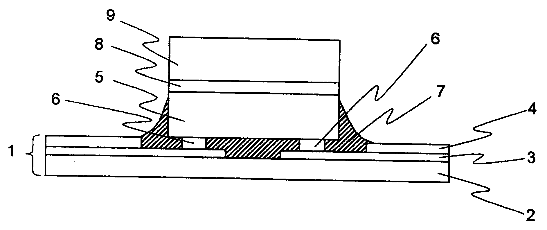
[0064]FIG. 1 shows a schematic sectional view of a COF semiconductor device with a heat spreader according to a first embodiment of the invention.

[0065] The COF semiconductor device with the heat spreader includes a flexible tape board 1 as an example of the tape board, a semiconductor element 5 mounted on the flexible tape board 1, and a heat spreader 9 mounted on the semiconductor element 5.

[0066] The flexible tape board 1 has a base film 2, interconnection lines 3 formed on the base film 2, and resist 4 formed on the interconnection lines 3. The resist 4 is so formed as not to cover part of the interconnection lines 3. It is noted that the interconnection lines 3 are an example of the interconnection pattern.

[0067] Bump electrodes 6 made of, for example, gold are formed on a front face of the semiconductor element 5. On the other hand, a heat spreader 9 is bonded via a die bond sheet 8 to the rear face of the semiconductor element 5 (a surface of the semiconductor element oppo...

second embodiment

[0080]FIG. 4 shows a schematic sectional view of a COF semiconductor device with a heat spreader according to a second embodiment of the invention.

[0081] The COF semiconductor device with the heat spreader includes a flexible tape board 1 as an example of the tape board, a semiconductor element 5 mounted on the flexible tape board 1, and a heat spreader 29 mounted on the semiconductor element 5. This heat spreader 29 functions as the heat spreader.

[0082] The flexible tape board 1 has a base film 2, interconnection lines 3 formed on the base film 2, and resist 4 formed on the interconnection lines 3. The resist 4 is so formed as not to cover part of the interconnection lines 3. It is noted that the interconnection lines 3 are an example of the interconnection pattern.

[0083] Bump electrodes 6 made of, for example, gold are formed on a front face of the semiconductor element 5. On the other hand, a heat spreader 29 is bonded via a die bond sheet 8 to the rear face of the semiconduct...


PUM

PropertyMeasurementUnit
thermal conductivityaaaaaaaaaa
areaaaaaaaaaaa
thicknessaaaaaaaaaa

Abstract

The semiconductor device of the invention has a heat spreader 9 mounted on a semiconductor element 5. The area of one surface of the heat spreader 9 closer to the semiconductor element 5 is generally equal to the area of one surface of the semiconductor element 5 closer to the heat spreader 9. With this structure, manufacturing cost of the semiconductor device can be reduced and moreover its reliability can be enhanced.

Description

CROSS-REFERENCE TO RELATED APPLICATIONS [0001] The present non-provisional application claims priority based on JP 2005-079167 applied for patent in Japan on Mar. 18, 2005 under U.S. Code, Volume 35, Chapter 119(a). The disclosure of the application is fully incorporated herein by reference. BACKGROUND OF THE INVENTION [0002] The present invention relates to a semiconductor device and a manufacturing method therefor. [0003] Conventionally, there has been provided a semiconductor device which adopts TCP (Tape Carrier Package) fabricated by TAB (Tape Automated Bonding) technique (see, for example, JP H5-160194 A). In this semiconductor device, a heat spreader is provided on a rear face of a semiconductor element (the rear face being opposite to the front face of the semiconductor element on which bumps are formed) for efficient radiation of heat generated by operations of the semiconductor element. [0004] A COF (Chip On Film) semiconductor device equipped with a heat spreader, which i...

Claims


Application Information

Patent Timeline
Patent Type & Authority Applications(United States)
IPC IPC(8): H05K7/20
CPCH01L21/563H01L23/36H01L2224/73203H01L2924/01004H01L2924/01078H01L2924/01079H01L2224/16225H01L2224/32225H01L2224/73204H01L2224/73253H01L2924/01019H01L2924/00H01L2924/00011H01L2924/00014H01L2224/0401D06C3/04D06C25/00D06C27/00
Inventor KATOH, TATSUYA
Owner SHARP KK
Why Eureka
Try Eureka