Non-volatile memory and method of fabricating the same

Inactive Publication Date: 2006-09-21
POWERCHIP SEMICON CORP
View PDF8 Cites 2 Cited by
  • Summary
  • Abstract
  • Description
  • Claims
  • Application Information

AI Technical Summary

Benefits of technology

[0010] Therefore, it is an object of the present invention to provide a method for fabricating a non-volatile memory. The method prevents the encroach problem from happening in the dielectric layer of the non-volatile memory. Accordingly, the quality of the film layer in the dielectric layer is improved, and the breakdown problem in device is eliminated, such that the reliability of the fabricating process is further improved.
[0011] It is another object of the present invention to provide a non-volatile memory, which provides an improved performance and write-in efficiency for the device.
[0026] The method for fabricating the non-volatile memory provided by the present invention forms a dielectric layer on the substrate, and the surface profile of the dielectric layer is presented in a ladder-like form. Thus, the film layer of the dielectric layer on a portion of the substrate closing to the sidewall of the semiconductor device is thicker. A higher resistance will be generated when a bias is provided, such that a higher electric field is generated in the channel below the dielectric layer with a thicker film layer. Therefore, the electrons are accelerated and the write-in efficiency of the device is effectively improved. In addition, since in the step of continuously removing a portion of the first dielectric layer until the surface of the substrate is exposed, the time spent in the wet etching fabricating process to expose the surface of the substrate is shorter, thus the encroach phenomenon occurred in the dielectric layer of the semiconductor device resulted from the erosion of the trench from the etching liquor is effectively eliminated. Accordingly, the quality of the film layer of the dielectric layer in the semiconductor device is improved, and the performance of the device and the reliability of the fabricating process are both improved. In addition, since the film layer of the dielectric layer between the semiconductor device and the first conductive layer is thicker, the breakdown problem is effectively eliminated and the performance of the device will not be affected.

Problems solved by technology

However, the method for fabricating the non-volatile memory mentioned above has some drawbacks.
For example, the write-in efficiency of the memory device is poor.
In addition, in the step of etching the dielectric material layer 102, an encroach problem may be occurred in the dielectric layer of the semiconductor device 101 due to over etching, which deteriorates the reliability of the device.
Similarly, in the step of etching the dielectric material layer 102, a breakdown problem may be occurred in the semiconductor device 101 and the word line due to over etching, which also seriously affects the performance of the device.

Method used


Image

  • Non-volatile memory and method of fabricating the same
  • Non-volatile memory and method of fabricating the same
  • Non-volatile memory and method of fabricating the same

Examples


Embodiment Construction

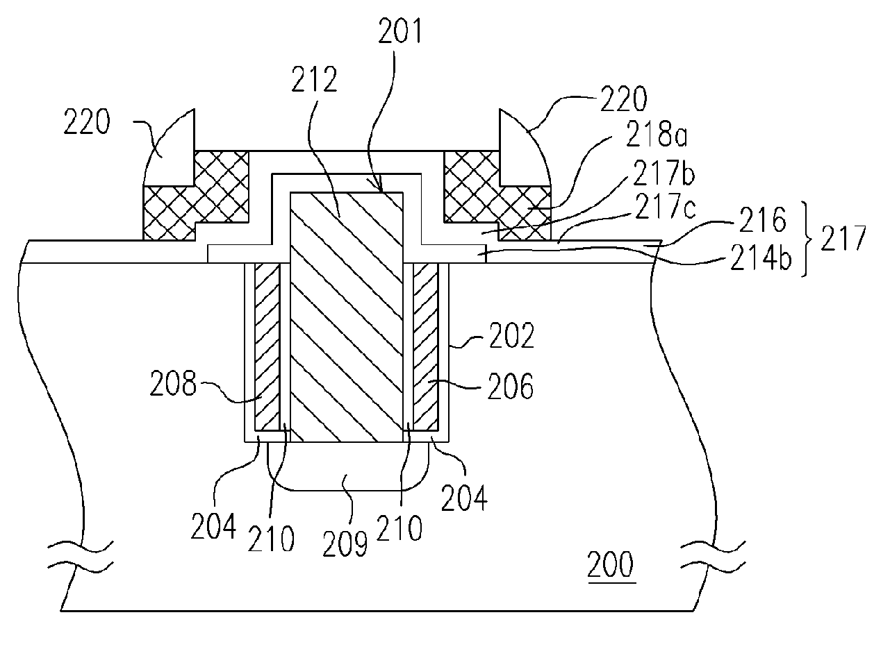
[0030]FIGS. 2A through 2J schematically show sectional views of fabricating a non-volatile memory according to a preferred embodiment of the present invention.

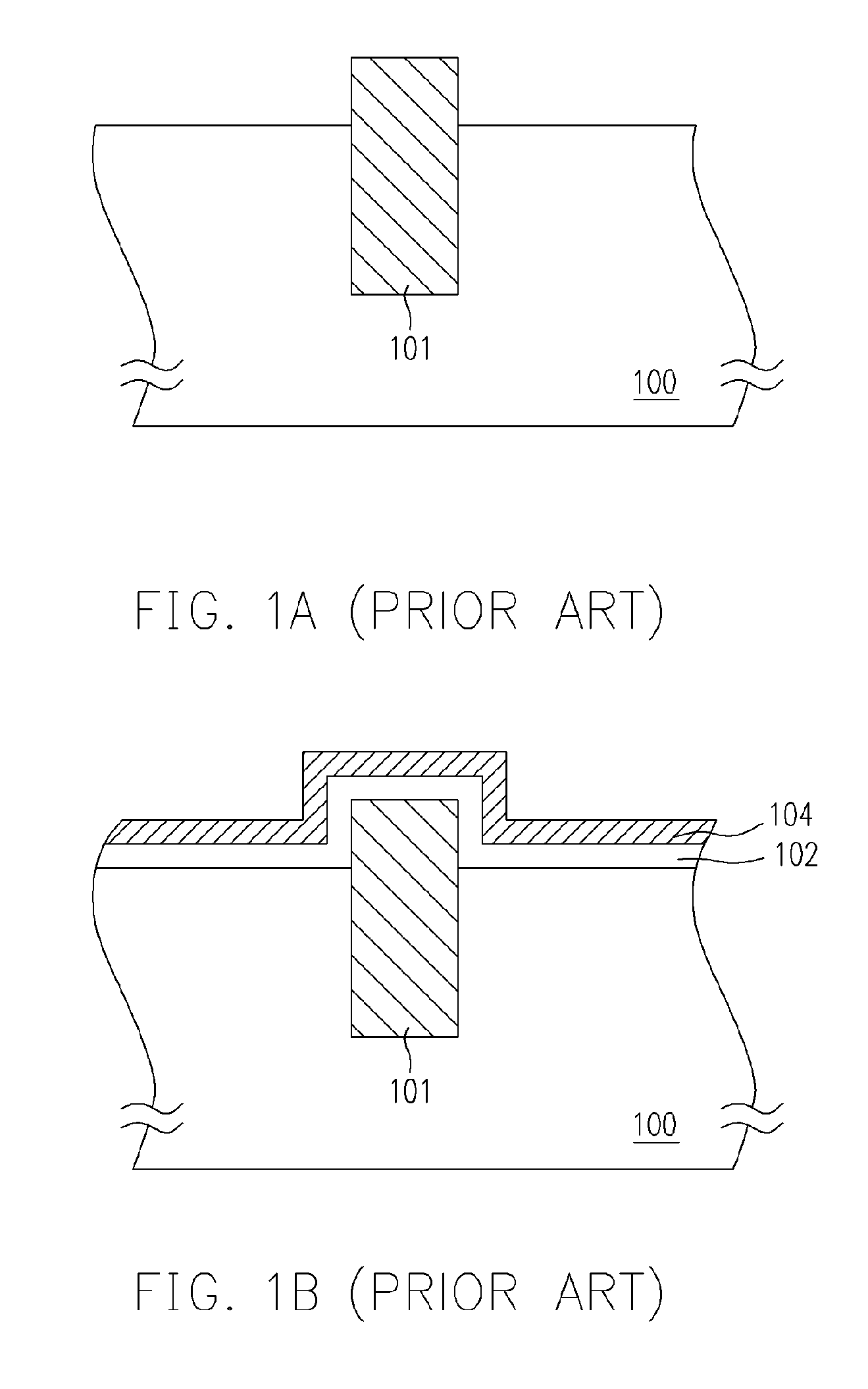
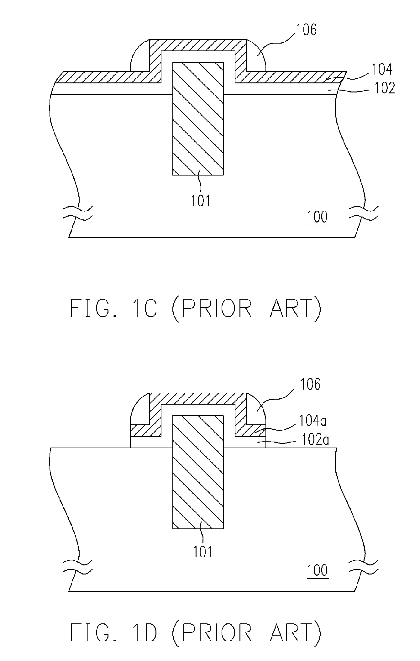
[0031] First, referring to FIG. 2A, a substrate 200 is provided. The substrate 200 is for example a silicon substrate, and a trench 202 is formed in the substrate 200. Wherein, the method for forming the trench 202 for example includes the following steps. First, a patterned mask material layer (not shown) is formed on the substrate 200, and the patterned mask material layer is for example made of a material such as silicon nitride and formed by the chemical vapor deposition method. Then, the patterned mask material layer is used as a mask to etch the substrate 200.

[0032] Then, referring to FIG. 2B, a tunnel oxide layer 204 is formed on the surface of the trench 202. The tunnel oxide layer 204 is for example made of a material such as silicon oxide and formed by a thermal oxidation method.

[0033] Afterwards, a conductive lay...


PUM


Abstract

A method for fabricating a non-volatile memory is disclosed. First, a semiconductor device is formed in a substrate, and the top of the semiconductor device is higher than the surface of the substrate. Then, a first dielectric layer is formed on the substrate, and the first dielectric layer covers the semiconductor device and the substrate. A portion of the first dielectric layer is removed so as to retain a portion of the first dielectric layer on the sidewall of the semiconductor device and the substrate. Afterwards, a second dielectric layer and a conductive layer are sequentially formed on the substrate, and a corresponding pair of mask spacers is formed on the conductive layer disposed on the sidewall of the semiconductor device. Finally, the mask spacers are used as an etching mask to continuously etch a portion of the conductive layer until the surface of the second dielectric layer is exposed.

Description

CROSS-REFERENCE TO RELATED APPLICATION [0001] This application claims the priority benefit of Taiwan application serial no. 94108315, filed on Mar. 18, 2005. All disclosure of the Taiwan application is incorporated herein by reference. BACKGROUND OF THE INVENTION [0002] 1. Field of the Invention [0003] The present invention relates to a semiconductor device and a method for fabricating the same, and more particularly, to a non-volatile memory and a method for fabricating the same. [0004] 2. Description of the Related Art [0005] Memory, like its name, is a semiconductor device for storing information and data. Since it is an advantage of the non-volatile memory that the stored data is not lost even when the power is shut down, the non-volatile memory has become an indispensable component in various electronic products that the normal operation of the electronic products can be ensured. In addition, the non-volatile memory has become a widely accepted memory device in the personal com...

Claims


Application Information

Patent Timeline
IPC IPC(8): H01L21/336
CPCH01L21/28273H01L29/66825H01L29/7881H01L29/40114
Inventor HUANG, MIN-SANCHEN, DAH-CHUANLAI, LIANG-CHUAN
Owner POWERCHIP SEMICON CORP
Why Eureka
Try Eureka