Verification circuitry for master-slave system
a verification circuit and masterslave technology, applied in the field of circuitry, can solve the problems of inability to conduct a realistic test of a system function that involves a continuous sequence of operations, no one master is capable of performing all the types of bus access, and the time required to execute the simulation becomes prohibitive, so as to simplify the testing of complex systems
- Summary
- Abstract
- Description
- Claims
- Application Information
AI Technical Summary
Benefits of technology
Problems solved by technology
Method used
Image

Examples
first embodiment
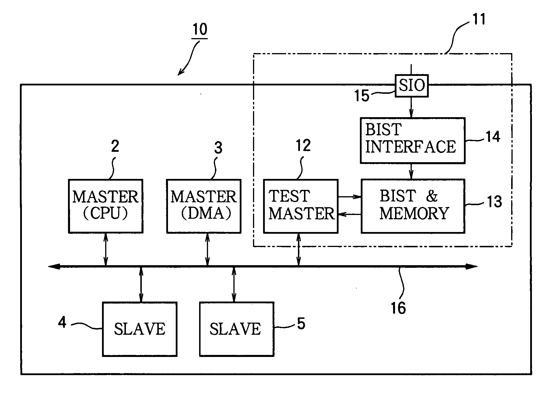
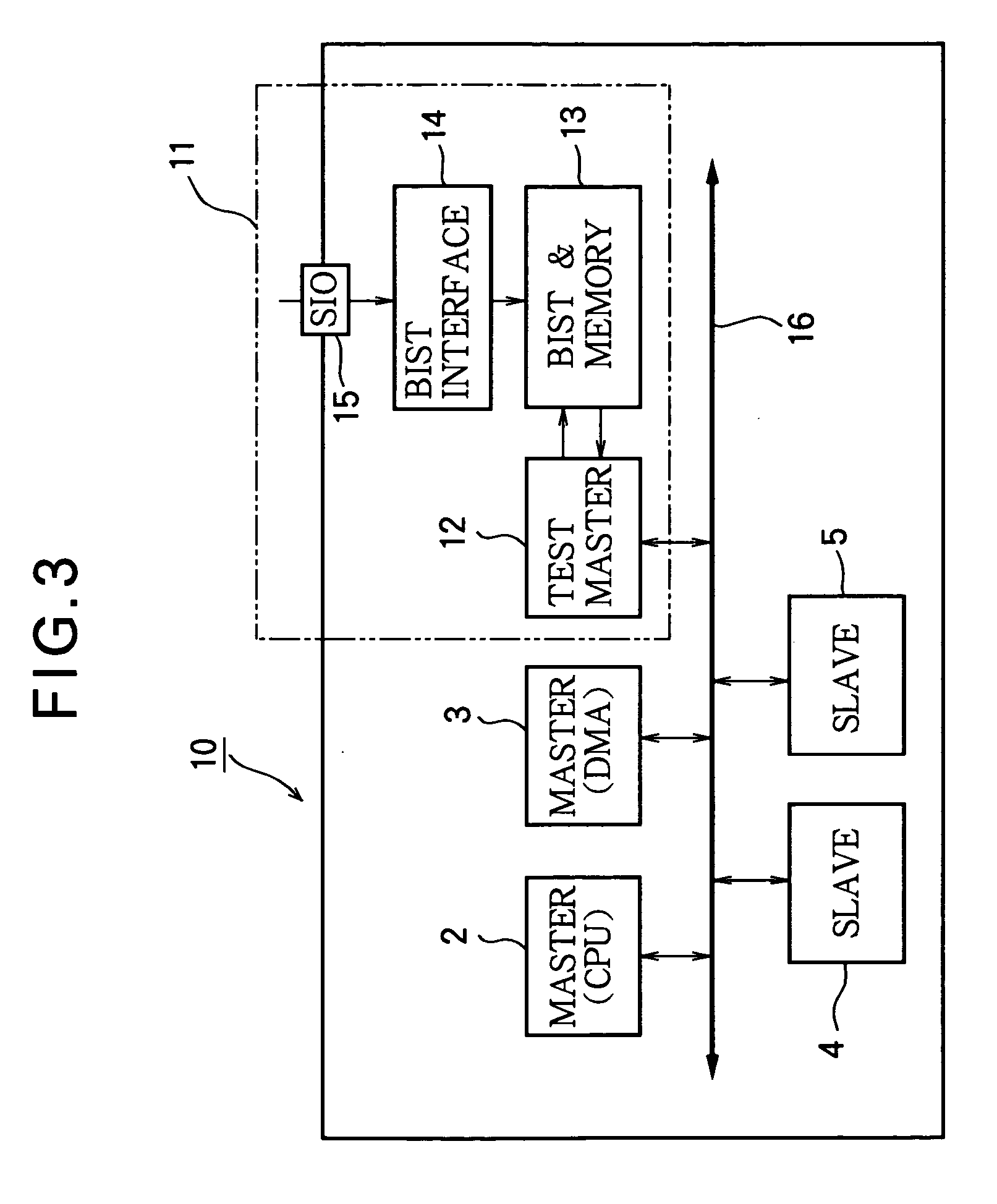
[0032] As a first embodiment, FIG. 3 shows a monolithic integrated circuit, more specifically an FPGA 10, including a CPU 2 and a DMA device 3 which operate as master devices, a pair of slave devices 4, 5, and system verification circuitry 11 embodying the present invention. The system verification circuitry 11 includes a test master circuit 12, a built-in self-test (BIST) and memory circuit 13, a built-in self-test interface circuit 14, and a serial interface 15. The test master circuit 12 is connected to the system bus 16 and operates as a master device to access the slave devices 4, 5 in the same way that the CPU 2 and DMA device 3 access them. If necessary, the test master circuit 12 can also access the DMA device 3 and CPU 2.
[0033] The system bus 16 interconnects the master devices 2, 3, 12 and slaves devices 3, 4 in the FPGA 10. The protocol used on the system bus 16 is illustrated in FIG. 4. Bus transfers are synchronized with a clock signal (clk). A master device outputs ad...
second embodiment
[0047] Referring to FIG. 5, the FPGA 50 in the second embodiment has the same master devices 2, 3 and slave devices 4, 5 as the first embodiment, and the system verification circuitry 51 in the second embodiment has the same test master circuit 12 and built-in self-test and memory circuit 13, but the built-in self-test interface circuit 52 is now connected to the system bus 16, and the system bus 16 is connected to an external memory 53 and I / O interface device 54. The FPGA 50, memory device 53, and I / O interface device 54 are mounted on a prototype printed circuit board.
[0048] The verification procedure is essentially the same as in the first embodiment, except that the host system downloads test patterns through the I / O interface device 54. The test patterns may be transferred from the I / O interface device 54 directly to the internal memory 13a (shown in FIG. 5) of the built-in self-test and memory circuit 13 in the FPGA 50 over the system bus 16, or may be first stored in the me...
PUM
 Abstract
Description
Claims
Application Information