
Method of increasing data setup and hold margin in case of non-symmetrical PVT

a data setup and data margin technology, applied in the field of memory devices, can solve the problems of data setup and hold time, dqs signal delay, rc delay of routing wires, transition delay of driver blocks b, etc., and achieve the effect of reducing duty cycle distortion in dram devices

Inactive Publication Date: 2006-09-28
INFINEON TECH AG
View PDF7 Cites 10 Cited by
  • Summary
  • Abstract
  • Description
  • Claims
  • Application Information

AI Technical Summary

Benefits of technology

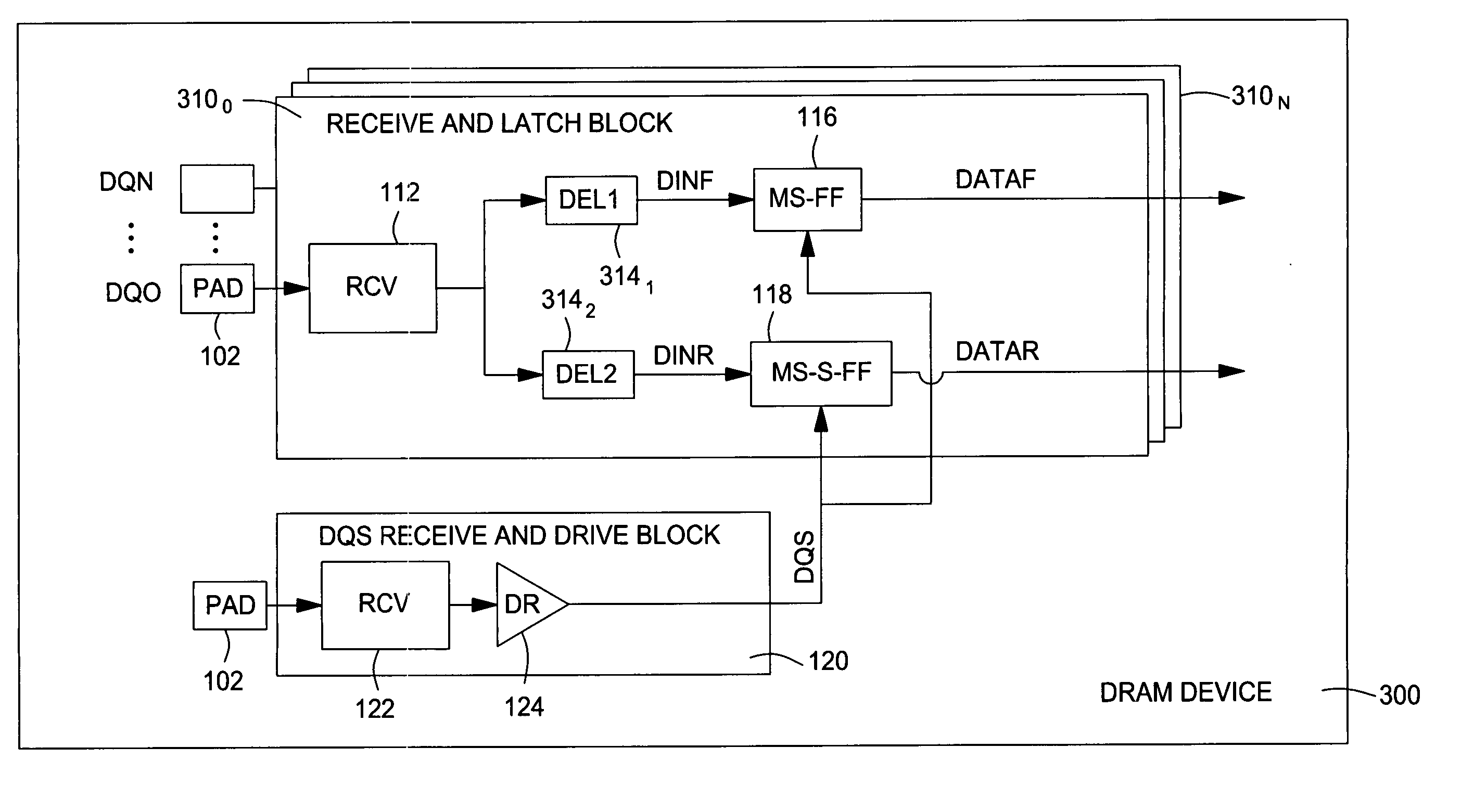
[0017] Embodiments of the invention generally provide techniques and apparatus to reduce duty cycle distortion in DRAM devices caused by process variations.

Problems solved by technology

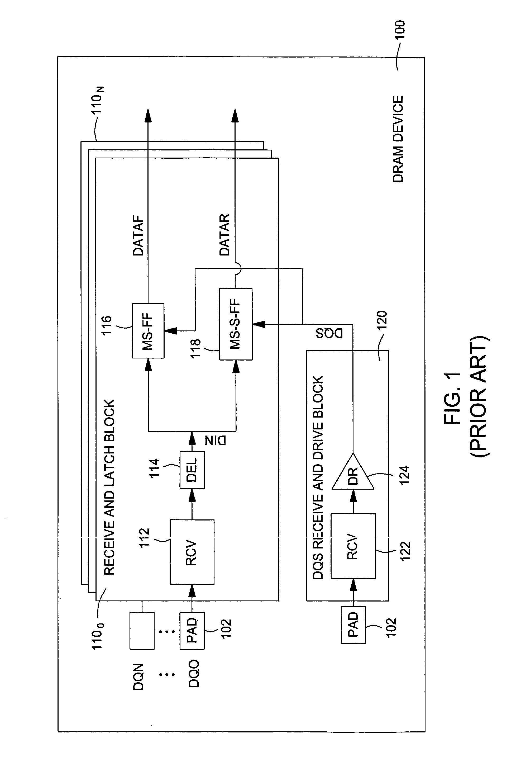
The delay on the DQS signal results from both RC delay of the routing wires and transition delay of the driver block 120.
Unfortunately, as DDR SDRAMS are run at increasingly higher frequencies and lower supply voltages, shrinking cycle times allow less for time for data setup and hold.
Further, as the operating frequencies increase, the processes with which these devices are built continue to shrink the feature size.
With decreasing feature size, process, voltage and temperature (PVT) deviations resulting in duty cycle distortion (e.g., due to differences in P and N type processes) become more pronounced.
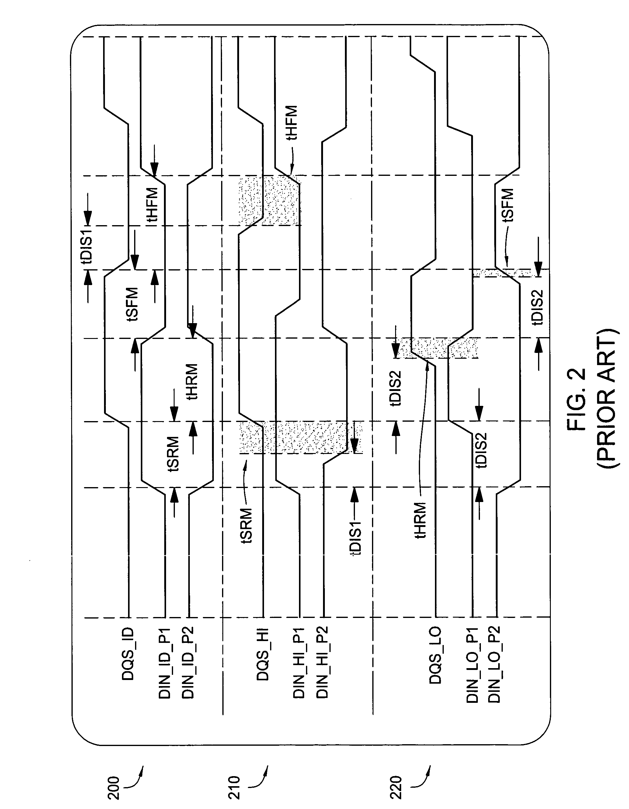
If the delay for rising and failing edges is affected differently from the PVT variations, the duty cycle is distorted.
While these margins may be acceptable in the example, in other cases the margins due to imbalance may be too narrow.
As illustrated, the delayed switching of the rising edge of the DQS signal results in insufficient hold timing margins (tHRM) before the falling edge of P1 (DIN_LO_P1).
Further, assuming the rising edge of P2 (DIN_LO_P2) will be delayed in a similar manner, setup timing margins (tSFM) for the rising edge of P2 prior to the falling edge of DQS may also be insufficient.
However, disadvantages to this approach include higher power consumption and larger area needed for the receiver blocks.
Particularly for low power derivates of DDR SDRAMs (e.g., Mobile DDR SDRAMs), power consumption of the data and DQS receiver blocks is critical.

Method used


Image

  • Method of increasing data setup and hold margin in case of non-symmetrical PVT
  • Method of increasing data setup and hold margin in case of non-symmetrical PVT
  • Method of increasing data setup and hold margin in case of non-symmetrical PVT

Examples


Embodiment Construction

[0028] Embodiments of the invention generally provide techniques and apparatus to reduce duty cycle distortion in DRAM devices, for example, caused by process variations. By dividing the undelayed output signal from the data receivers into two separate paths and providing independently adjustable delay blocks in each path leading to the rising and falling edge data latches, the setup and hold timing margins may be increased.

[0029] Embodiments of the present invention are described below with reference to double data rate (DDR) DRAM devices in which two bits of data are exchanged on each data pad in each clock cycle (i.e., on rising and falling edges). Those skilled in the art will appreciate, however, that the concepts described herein may be applied to virtually any device where data is transferred synchronously (e.g., on both edges of a clock). For example, the concepts described herein may also be applied to advantage to adjust timing margins in devices in which more than two bi...


PUM


Abstract

Techniques and apparatus to reduce duty cycle distortion in DRAM devices caused by process variations are provided. By dividing the undelayed output signal from the data receivers into two separate paths and providing independently adjustable delay blocks in each path leading to the rising and falling edge data latches, the setup and / or hold timing margins may be adjusted.

Description

BACKGROUND OF THE INVENTION [0001] 1. Field of the Invention [0002] The invention generally relates to memory devices and, more particularly to adjusting delay blocks to compensate for process variations. [0003] 2. Description of the Related Art [0004] The evolution of sub-micron CMOS technology has resulted in an increasing demand for high-speed semiconductor memory devices, such as dynamic random access memory (DRAM) devices, pseudo static random access memory (PSRAM) devices, and the like. Herein, such memory devices are collectively referred to as DRAM devices. [0005] Some types of DRAM devices have a synchronous interface, generally meaning that data is written to and read from the devices in conjunction with a clock pulse (e.g., a data strobe signal DQS). Early synchronous DRAM (SDRAM) devices transferred a single bit of data per clock cycle (e.g., on a rising edge) and are appropriately referred to as single data rate (SDR) SDRAM devices. Later developed double-data rate (DDR...

Claims


Application Information

Patent Timeline
Patent Type & Authority Applications(United States)
IPC IPC(8): G11C7/00
CPCG11C7/1078G11C7/1087G11C7/1093G11C7/22G11C11/4076G11C11/4096G11C2207/2254
Inventor PARTSCH, TORSTEN
Owner INFINEON TECH AG
Learn More