High-voltage field effect transistor having isolation structure

a transistor and isolation structure technology, applied in the field of metal oxide semiconductor field effect transistors, can solve the problems of interference to the control circuit, transistor current may produce ground bounce, and the transistor without isolation structure is not suitable for the integrated technology

Inactive Publication Date: 2006-10-05
FAIRCHILD TAIWAN
View PDF6 Cites 5 Cited by
  • Summary
  • Abstract
  • Description
  • Claims
  • Application Information

AI Technical Summary

Benefits of technology

[0005] Accordingly, to overcome the above disadvantages, the present invention provides a field effect transistor device having higher breakdown voltage, lower conductive resistance and an isolation structure for integrating a monolithic IC.
[0011] Furthermore, the first deep N-type well and the second deep N-type well respectively formed by the first N-type diffusion region and the second diffusion region provide a low-resistance path which limits the transistor current between the drain region and the source region.

Problems solved by technology

However, the high-voltage transistor fabricated in current standard process does not have an isolation structure, and the transistor current without isolation structure may flow in the substrate and cause disturbance to the control circuit.
Also, the transistor current may produce ground bounce to affect the control signal of the control circuit.
Accordingly, the transistor without the isolation structure is not suitable for the integrated technology.
In a conventional technology, a thin epitaxial layer and an N-type buried layer are used to provide the transistor an isolation structure and high breakdown voltage, but the complicated manufacturing process increases the fabricating cost and reduces the yield.

Method used


Image

  • High-voltage field effect transistor having isolation structure
  • High-voltage field effect transistor having isolation structure
  • High-voltage field effect transistor having isolation structure

Examples


Embodiment Construction

[0019] Reference will now be made in detail to the present embodiments of the invention, examples of which are illustrated in the accompanying drawings. Wherever possible, the same reference numbers are used in the drawings and the description to refer to the same or like parts.

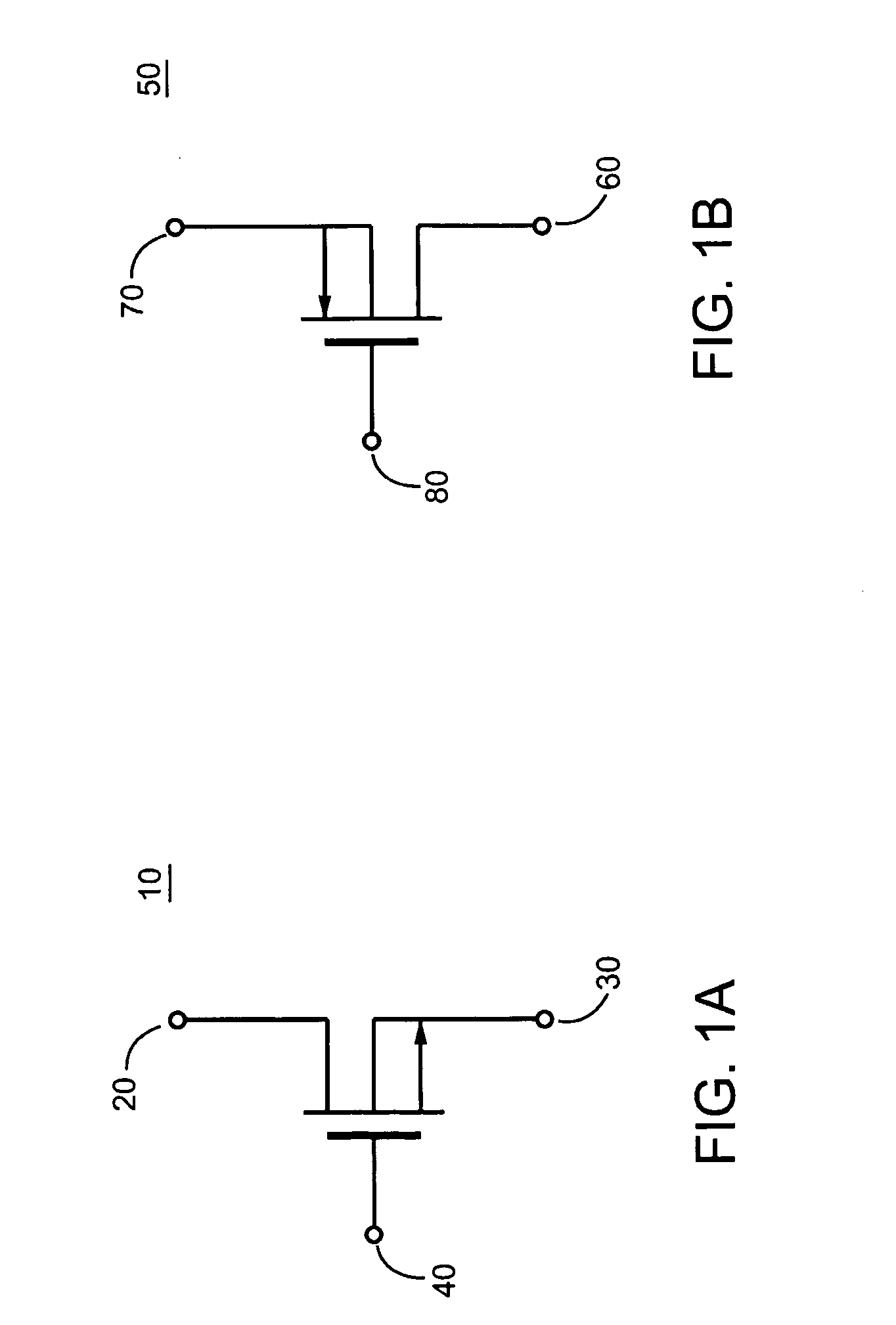
[0020]FIG. 1A is a diagram showing an N-type MOSFET 10, comprising a drain 20, a source 30, and a polysilicon gate 40. FIG. 1B is a diagram showing a P-type MOSFET 50, comprising a drain 60, a source 70 and a polysilicon gate 80.

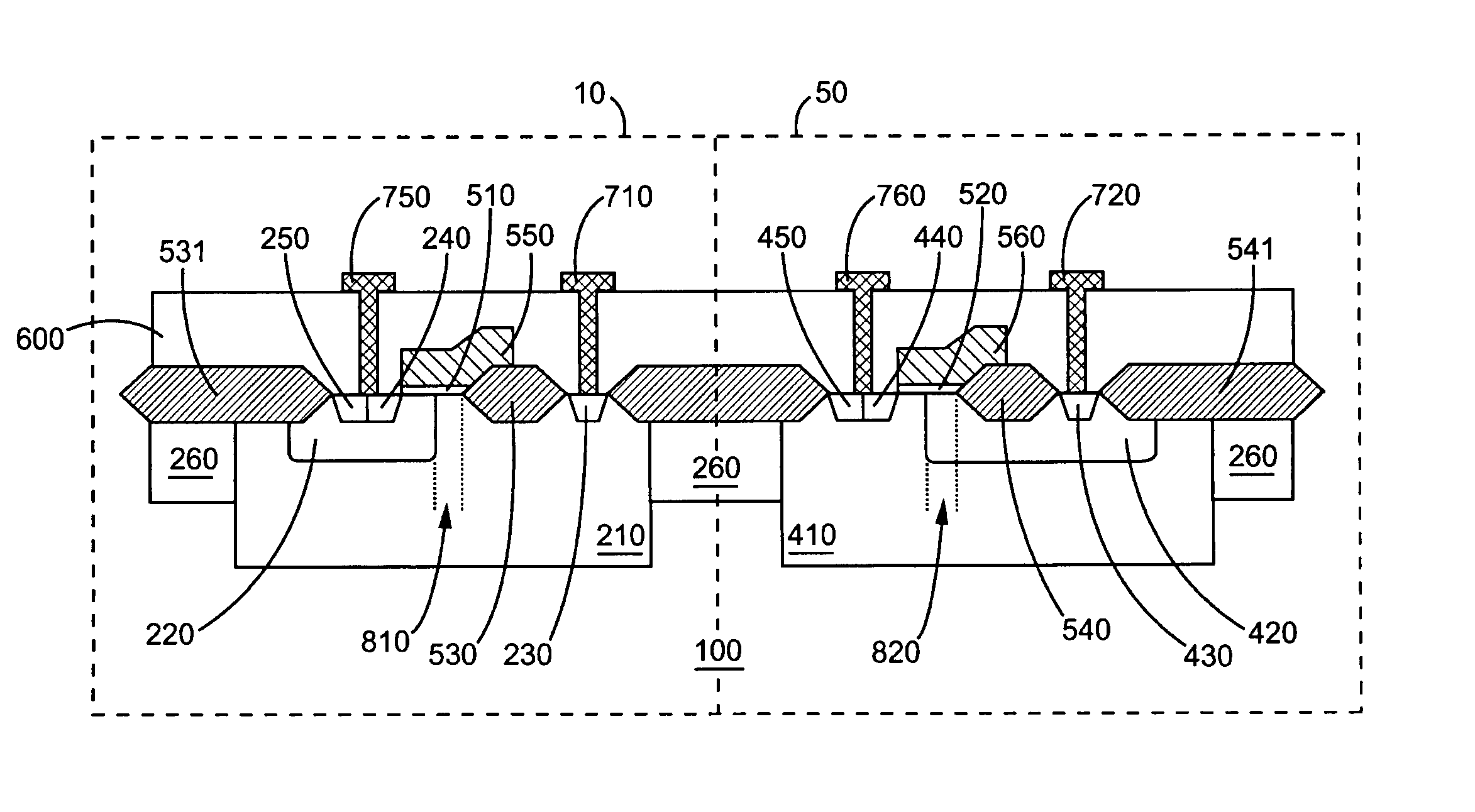
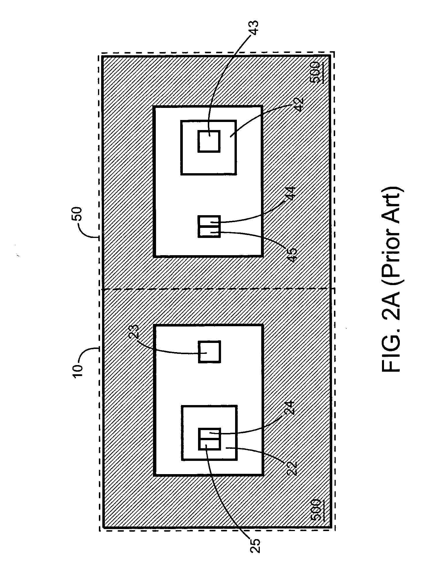
[0021]FIG. 2A is a top view showing a conventional high-voltage transistor device, comprising an N-type MOSFET 10 and a P-type MOSFET 50. FIG. 3A is a side view showing a conventional high-voltage transistor device having an isolation structure. As shown in FIG. 2A and FIG. 3A, the N-type MOSFET 10 and P-type MOSFET 50 include a P-type substrate 100, an N+-type buried layer 860 and a P+-type buried layer 880 formed in the P-type substrate 100, an N-type epitaxial layer 660 and an N-...


PUM


Abstract

A high-voltage MOSFET having isolation structure is provided. An N-type MOSFET includes a first deep N-type well. A first P-type region is formed in the first deep N-type well to enclose a first source region and a first contact region. A first drain region is formed in the first deep N-type well. A P-type MOSFET includes a second deep N-type well. A second P-type region is formed in the second deep N-type well to enclose a second drain region. A second source region and a second contact region are formed in the second deep N-type well. A polysilicon gate oxidation layer is disposed above the thin gate oxidation layer and the thick field oxidation layer to control the current in the channel of the MOSFET. Separated P-type regions provide further isolation between MOSFETs. A first gap and a second gap increase the breakdown voltage of the high-voltage MOSFET.

Description

BACKGROUND OF THE INVENTION [0001] 1. Field of the Invention [0002] The present invention relates to a semiconductor device. More particularly, the present invention relates to a metal oxide semiconductor field effect transistor (MOSFET). [0003] 2. Description of the Related Art [0004] To integrate control circuits and high-voltage transistors has become a development trend for present power integrated circuit (Power IC). Therefore, if high-voltage transistor devices can be fabricated using standard process, it would be a preferable way for integrating a monolithic IC. However, the high-voltage transistor fabricated in current standard process does not have an isolation structure, and the transistor current without isolation structure may flow in the substrate and cause disturbance to the control circuit. Also, the transistor current may produce ground bounce to affect the control signal of the control circuit. Accordingly, the transistor without the isolation structure is not suita...

Claims


Application Information

Patent Timeline
Patent Type & Authority Applications(United States)
IPC IPC(8): H01L29/00
CPCH01L21/823418H01L21/823493H01L29/7816H01L29/42368H01L29/66681H01L29/0696
Inventor HUANG, CHIH-FENGCHIEN, TUO-HSINLIN, JENN-YU G.YANG, TA-YUNG
Owner FAIRCHILD TAIWAN
Why Eureka
Try Eureka