Apparatus for use in thinning a semiconductor workpiece

a technology for thinning semiconductor workpieces and workpieces, which is applied in mechanical apparatus, turning machine accessories, manufacturing tools, etc., can solve the problems of icds operating at extremely high speeds, prone to heat generation, and drawbacks of conventional back grinding processes, etc., and achieves thinning semiconductor wafers. , the effect of less susceptible to breakage and resistance to bowing and warping

Inactive Publication Date: 2006-10-05
SEMITOOL INC
View PDF0 Cites 6 Cited by
  • Summary
  • Abstract
  • Description
  • Claims
  • Application Information

AI Technical Summary

Benefits of technology

[0010] The present invention provides a chuck for use in processing semiconductor wafers. By utilizing the chuck of the present invention, it is possible to produce thinner semiconductor wafers that at the same time remain strong and resistant to bowing and warping. As a result, the wafers produced by the present process are less susceptible to breakage. The process and equipment of the present invention also offers an improved product structure for handling thinned wafers, while reducing the number of processing steps. This results in, among other things, improved yields and improved process efficiency.
[0011] The chuck of the present invention receives and supports a semiconductor workpiece having a device side, a bevel and a back side. The chuck has a body for supporting the workpiece, a retainer removeably attached to the body and adapted to cover a peripheral portion of the back side of the workpiece, and at least one member for creating a seal between the retainer and the back side of the workpiece. During processing, the seal prevents process fluid from contacting: (i) the periphery of the back side of the workpiece; (ii) the bevel of the workpiece; and (iii) the device side of the workpiece. It has been discovered that during the wet chemical etching, process fluid can build up at the interface between the seal member and the workpiece. The buildup of process fluid at the seal interface can, in some instances, result in a variation in the etching rate and in the thickness of the workpiece. Accordingly, it is advantageous to facilitate distribution of fresh process fluid across the entire back side of the workpiece, and in particularly at the point of contact between the sealing member and the workpiece.
[0012] The chuck of the present invention includes a seal member that helps facilitate flow or distribution of fresh process fluid at the seal interface. In one aspect of the present invention, the chuck comprises a body for supporting the workpiece and a removable retainer. The retainer can be attached to the body and is adapted to cover a peripheral portion of the back side of the workpiece. The chuck includes a compressible member for forming a seal between the retainer and the back side of the workpiece. The seal member has a surface that slopes downwardly towards the workpiece to create an angle at a point of contact with the workpiece. In one embodiment, the angle between the seal member and the workpiece is 90 degrees or more. Due to the angle between the seal member and the workpiece, fresh process fluid is continuously distributed to this area of the workpiece, resulting in a greater process uniformity across a greater portion of the back side of the workpiece.
[0014] The present invention also provides several processes for thinning a semiconductor workpiece. In one aspect, the process includes the steps of placing the semiconductor workpiece into a chuck adapted to cover a peripheral portion of the back side of the workpiece, leaving approximately 95% of the back side surface of the workpiece exposed. The semiconductor workpiece is then thinned via a wet chemical etching process wherein the back side of the workpiece is exposed to an oxidizing agent (e.g., HF, HNO3, H3PO4, H2SO4) or alternatively to a caustic solution (e.g., KOH, NaOH, H2O2). During the wet chemical etching step, the exposed back side of the workpiece is thinned to a thickness less than 50% of the pre-wet chemical etching thickness of the workpiece. Due to the configuration of the chuck, a rim is formed at the periphery of the workpiece, or as it is commonly referred to in the industry, the “exclusion zone.” The rim has a thickness approximately equal to the thickness of the workpiece prior to the wet chemical etch step (e.g., in a range of 600 to 725 microns). The remainder of the workpiece (i.e., the thinned main body) has a thickness less than 50% of the rim thickness (e.g., less than 300 microns, preferably less than 125 microns, more preferably less than 100 microns, especially less than 50 microns and even less than 25 microns). The relatively thicker rim provides strength to the thinned workpiece and permits the workpiece to be handled for additional processing with conventional automated handling equipment. This process eliminates the limitations associated with known methods of thinning semiconductor workpieces mentioned above, while increasing overall manufacturing efficiencies.

Problems solved by technology

In addition, advanced packaging of semiconductor devices (e.g., stacked dies or “flip-chips”) provide dimensional packaging constraints which also require an ultra-thin die.
Moreover, as operating speeds of ICDs continue to increase heat dissipation becomes increasingly important.
This is in large part due to the fact that ICDs operated at extremely high speeds tend to generate large amounts of heat.
However, conventional back grinding processes have drawbacks.
Mechanical grinding induces stress in the surface and edge of the wafer, including micro-cracks and edge chipping.
This induced wafer stress can lead to performance degradation and wafer breakage resulting in low yield.
In addition, there is a limit to how much a semiconductor wafer can be thinned using a back grinding process.
Additionally, chemical etching after back grinding thins the semiconductor wafer beyond conventional back grinding capabilities.
Although methods for thinning semiconductor wafers are known, they are not without limitations.
For example, mounting a semiconductor wafer to a submount or “chuck” (as it is commonly known) so that the wafer can be thinned requires expensive coating and bonding equipment and materials, increased processing time, and the potential for introducing contaminates into the process area.
Additionally, adhesives for bonding a wafer to a chuck that may be useful in a mechanical grinding process will not withstand the chemical process fluids used in wet chemical etching.
Furthermore, the current use of a photoresist or adhesive tape fails to provide mechanical support for very thin wafers either during the back grind process or in subsequent handling and processing.
The use of tape also creates obstacles in the removal process.
For example, tape removal may subject a wafer to unwanted bending stresses.
In the case of a photoresist, the material is washed off the device side of a wafer with a solvent, adding to the processing time and use of chemicals, and increasing the risk of contamination.
The use of taping and protective polymers are also costly, since both equipment and materials are necessary to apply and remove the protective media.
Further, thinned semiconductor wafers are prone to warping and bowing.
And because thinned semiconductor wafers can be extremely brittle, they are also prone to breakage when handled during further processing.
Thinned semiconductor wafers (e.g., below 250 microns) also present complications in automated wafer handling because, in general, existing handling equipment has been designed to accommodate standard wafer thicknesses (e.g., 650 microns for 150 mm wafer and 725 microns for 200 and 300 mm wafers).

Method used


Image

  • Apparatus for use in thinning a semiconductor workpiece
  • Apparatus for use in thinning a semiconductor workpiece
  • Apparatus for use in thinning a semiconductor workpiece

Examples


Embodiment Construction

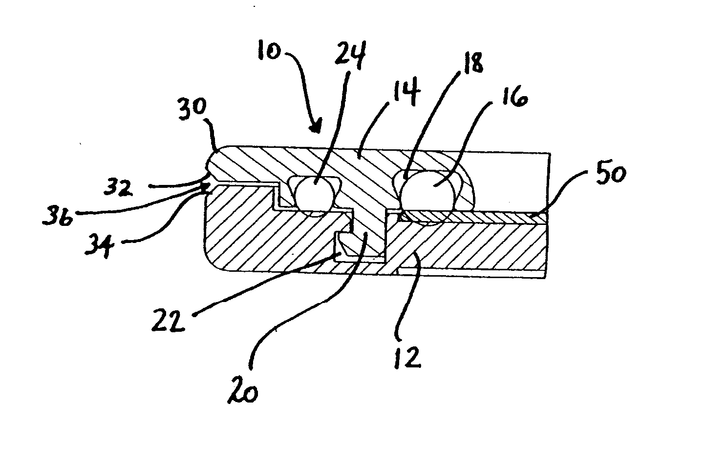
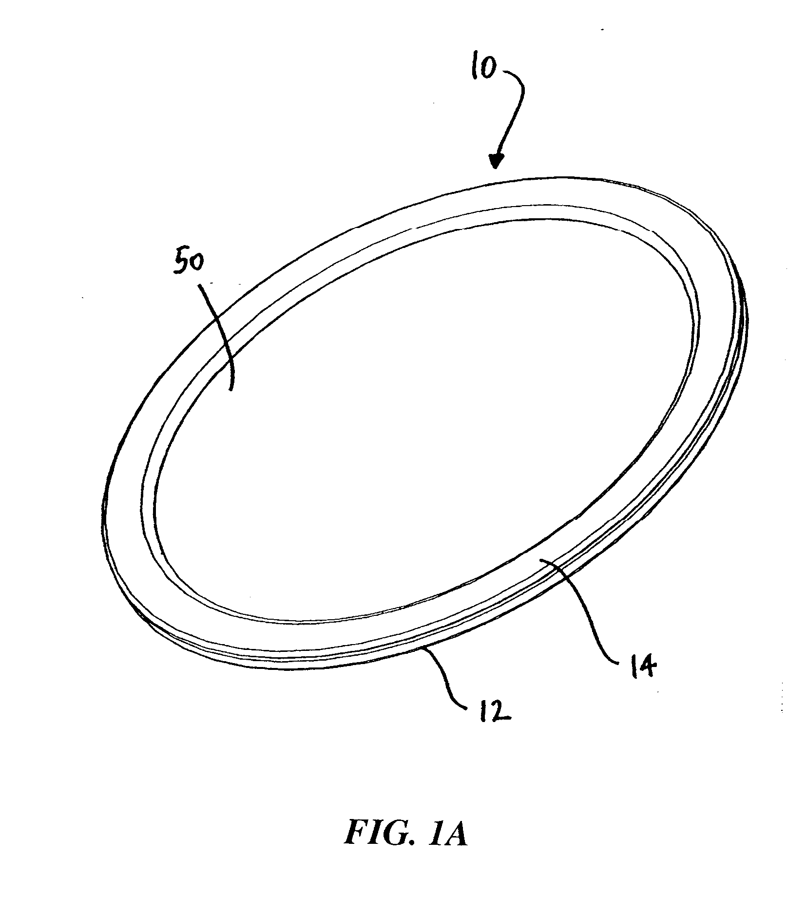
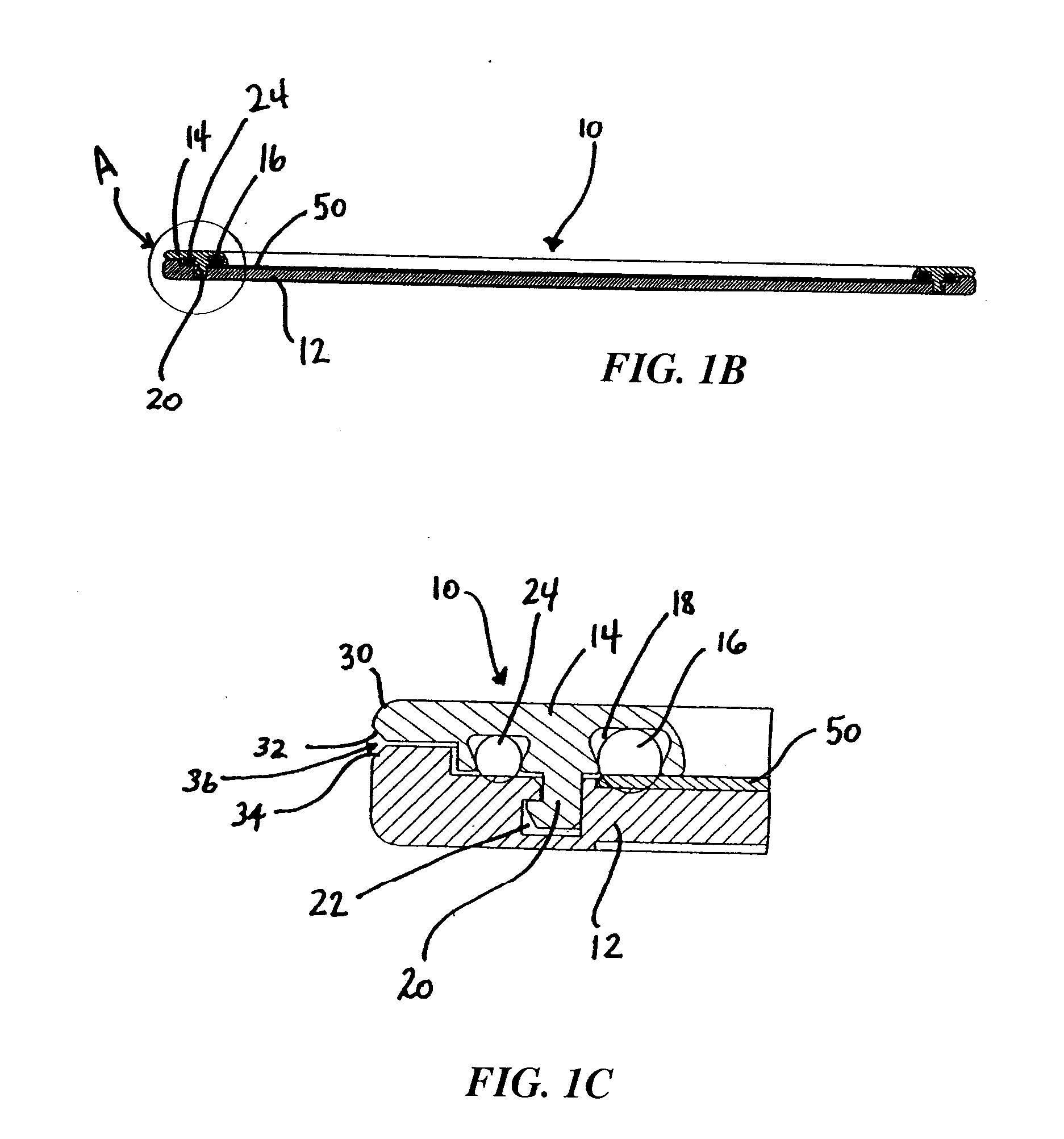
[0048] With reference to FIGS. 1A-1E, there is shown a chuck 10 for supporting a semiconductor workpiece 50 during processing in accordance with one embodiment of the present invention. The chuck 10 is comprised of a supporting body 12, a retainer 14 and a sealing members 16, 24. The retainer 14 has two grooves or recesses 18. The sealing members 16, 24 are housed in the annular grooves 18, respectively. The retainer 14 is preferably in the form of a ring and is removeably attached to the supporting body 12. In use, the workpiece 50, which has a device side 51, a bevel (i.e., peripheral edge) 52 and a back side 53, is placed onto a supporting surface 18 of the supporting body 12 of chuck 50, device side 51 down. The retainer 14 is then attached to the outer periphery of the supporting body 12. As shown specifically in FIG. 1C, when the retainer 14 is engaged to the supporting body 12, the retainer 14 wraps around the outer end of the supporting body 12 and covers a peripheral portio...


PUM


Abstract

The present invention provides an apparatus and method for use in processing semiconductor workpieces. The new apparatus and method allows for the production of thinner workpieces that at the same time remain strong. Particularly, a chuck is provided that includes a body, a retainer removeably attached to the body and a seal forming member. When a workpiece is placed on the chuck body and the retainer is engaged to the body, a peripheral portion of the back side of the workpiece is covered by the retainer while an interior region of the back side of the workpiece is exposed. The exposed back side of the workpiece is then subjected to a wet chemical etching process to thin the workpiece and form a relatively thick rim comprised of semiconductor material at the periphery of the workpiece. The thick rim or hoop imparts strength to the otherwise fragile, thinned semiconductor workpiece. Semiconductor workpieces made according to the present invention offer an improved structure for handling thinned wafers in conventional automated equipment. This results in improved yields and improved process efficiency.

Description

CROSS-REFERENCE TO RELATED APPLICATIONS [0001] This application is a continuation-in-part of U.S. application Ser. No. 10 / 923,436, filed on Aug. 20, 2004, and now pending, the entire disclosure of which is incorporated herein by reference. Priority to application Ser. No. 10 / 923,436 is claimed under 35 U.S.C. 119, 120 and / or 365.TECHNICAL FIELD [0002] The invention relates to a process and apparatus for use with workpieces, such as semiconductor wafers, flat panel displays, rigid disk or optical media, thin film heads or other workpieces formed from a substrate on which microelectronic circuits, data storage elements or layers, or micro-mechanical elements may be formed. These and similar articles are collectively referred to herein as a “wafer” or “workpiece.” Specifically, the present invention relates to a process and apparatus for use in thinning semiconductor workpieces. BACKGROUND OF THE INVENTION [0003] State of the art electronics (e.g., cellular phones, personal digital ass...

Claims


Application Information

Patent Timeline
Patent Type & Authority Applications(United States)
IPC IPC(8): B23B31/00
CPCH01L21/6835Y10T279/35H01L2221/6834
Inventor DOLECHEK, KERT L.THOMPSON, RAYMON F.
Owner SEMITOOL INC
Why Eureka
Try Eureka