Electrooptical apparatus and method of manufacturing electrooptical apparatus

a manufacturing method and electrooptical technology, applied in the manufacture of electrode systems, electric discharge tubes/lamps, discharge tubes luminescent screens, etc., can solve the problems of brightness unevenness, display unevenness, and liquid composition rapidly evaporated on the pixel electrode, and achieve high reproducibility and increase the electrical resistance of a region

Inactive Publication Date: 2006-10-05
SEIKO EPSON CORP
View PDF30 Cites 18 Cited by
  • Summary
  • Abstract
  • Description
  • Claims
  • Application Information

AI Technical Summary

Benefits of technology

[0041] By this structure, it is possible to increase the electrical resistance of a region onto which light is irradiated by irradiating the function layer and performing a heating treatment with high reproducibility.

Problems solved by technology

However, in the liquid droplet discharge method, the solvent in the liquid composition coated on the pixel electrode is rapidly evaporated.
The dry time difference between the liquid compositions causes unevenness in film thicknesses of layers of the organic EL element in a pixel or between pixels, and thus causes display unevenness such as brightness unevenness.
However, the dry state of the liquid composition is also affected by the surface state of the barrier rib.
Accordingly, although the dummy coating region is provided, if the surface state of the barrier rib is not uniform, it is difficult to form a uniform layer.

Method used


Image

  • Electrooptical apparatus and method of manufacturing electrooptical apparatus
  • Electrooptical apparatus and method of manufacturing electrooptical apparatus
  • Electrooptical apparatus and method of manufacturing electrooptical apparatus

Examples


second embodiment

[0088] Next, a second embodiment of the invention will be described with reference to FIG. 6. In the second embodiment, the same elements as those of the first embodiment are denoted by the same reference numerals and their detailed description will be omitted.

[0089]FIG. 6A is a front view of a light emission element array 22A according to a second embodiment, FIG. 6B is a cross-sectional view taken along line VIB-VIB of FIG. 6A, and FIG. 6C is a cross-sectional view taken along line VIC-VIC of FIG. 6A.

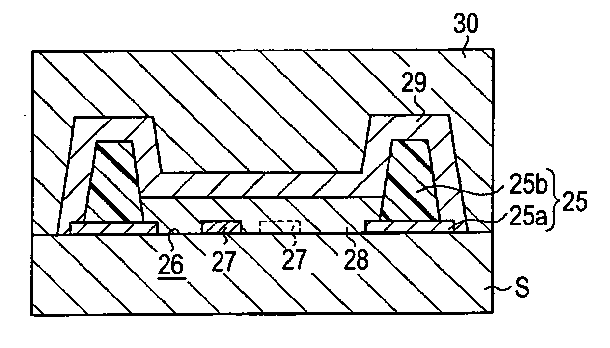
[0090] As shown in FIG. 6A, similar to the first embodiment, the light emission element array 22A includes a plurality of organic EL elements 24 arranged on a substrate S and a lyophobic bank 25b surrounds the whole of the light emission element array 22A. Meanwhile, in the present embodiment, a lyophilic bank 45 is disposed to define the pixel electrodes 27.

[0091] For example, the lyophilic bank 45 is formed of silicon oxide SiO2 at a film thickness of 50 to 150 nm. Alternatively,...

third embodiment

[0093] Next, a third embodiment of the invention will be described with reference to FIG. 7. In the third embodiment, the same elements as those of the first and second embodiments are denoted by the same reference numerals and their detailed description will be omitted.

[0094]FIG. 7 is a front view of a light emission element array 22B according to a third embodiment. As shown in FIG. 7, in the light emission element array 22B, one bank 50 is formed to surround the whole of a plurality of organic EL elements 24, similar to the first embodiment. In the light emission element array 22B, the shape of the bank 50 formed on a substrate S is different from that of the bank 25 of the first embodiment. That is, as shown in FIG. 7, in the present embodiment, the bank 50 is formed such that the inner shape of the concave region 26 at side of the center of the substrate corresponds to the shape of the pixel electrode 27 of the organic EL element 24. In the present embodiment, since the pixel ...

fourth embodiment

[0097] Next, a fourth embodiment of the invention will be described with reference to FIGS. 8 to 11. In the fourth embodiment, the same elements as those of the first embodiment are denoted by the same reference numerals and their detailed description will be omitted.

[0098]FIG. 8A is a front view of a light emission element array 22C according to a fourth embodiment, and FIG. 8B is a cross-sectional view taken along line VIIIB-VIIIB of FIG. 8A.

[0099] Each of organic EL elements 24 of the light emission element array 22C include a hole injection layer 61 and an electron injection layer 62, in addition to a light emission layer 28, as a function layer.

[0100] In more detail, as shown in FIG. 8B, the hole injection layer 61 is formed on the bottom of a concave region 26 to cover pixel electrodes 27. The hole injection layer 61 is made of a mixture of Poly-3,4-Ethylenedioxythiophene (hereinafter, referred to as “PEDOT”) and polystyrene sulfonic acid (hereinafter, referred to as “PSS”)...


PUM


Abstract

An electrooptical apparatus includes a light emission element array in which a plurality of light emission elements are arranged, and a barrier rib which surrounds the light emission element array.

Description

BACKGROUND [0001] 1. Technical Field [0002] The present invention relates to an electrooptical apparatus and a method of manufacturing the electrooptical apparatus. [0003] 2. Related Art [0004] Recently, as a light emission element, an electrooptical apparatus called an optical writing head of a display or a printer using an organic electroluminescence element (hereinafter, referred to as “organic EL element”) has been actively developed. [0005] A method of manufacturing an electrooptical apparatus varies depending on whether a light emission material composing the organic EL element (hereinafter, referred to as “organic EL material”) is a polymer organic material or a low molecular organic material. In addition, if the organic EL material is the polymer organic material, a liquid droplet discharge method of dissolving or dispersing the organic EL material in a specific solvent to form a liquid composition, discharging the liquid composition from a nozzle of a liquid droplet dischar...

Claims


Application Information

Patent Timeline
Patent Type & Authority Applications(United States)
IPC IPC(8): H05B33/00H05B33/10
CPCB41J2/45H01L27/3246H01L51/0005H01L51/5088H01L2251/5361H01L51/5203H01L51/5206H01L51/5237H01L51/5092H10K59/10H10K59/122H10K71/135H10K50/171H10K50/17H10K50/81H10K50/844H10K59/805D05C9/06H10K50/805
Inventor TANABE, SEIICHIMACHIDA, YOSHIHIKO
Owner SEIKO EPSON CORP
Why Eureka
Try Eureka