Organic electroluminescence device

Inactive Publication Date: 2006-10-05
SONY CORP
View PDF15 Cites 69 Cited by
  • Summary
  • Abstract
  • Description
  • Claims
  • Application Information

AI Technical Summary

Benefits of technology

[0012] Further, in JP-A No. 2004-296410 that discloses the third structure, the metal layer (electron injecting layer) is disposed in contact with the light emission layer that forms the organic layer. In this case, the electron injecting layer can not provide a hole blocking property as a function inherent to the layer. Then, holes can not be confined sufficiently in the light emission layer to decrease the probability of re-combination between holes and electrons in the light emission layer. Accordingly, light emission efficiency is lowered. Further, since the metal layer (electron injection layer) is disposed in contact with the light emission layer that forms the organic layer, the electron transportability incre

Problems solved by technology

This can no more ensure a sufficient electron injecting efficiency from the electron injecting layer to the organic layer and no sufficient life can be obtained compared with a device of using a not-transparent cathode (for example, Mg—Ag alloy, Al, etc. of a thick film of about 100 nm).
However, since the metal layer is not oxidized as a result, light absorption inherent to the metal remains and possibly making it difficult to ensure light transmittance.
In this case, the electron injecting layer can not provide a hole blocking property as a function i

Method used


Image

  • Organic electroluminescence device
  • Organic electroluminescence device
  • Organic electroluminescence device

Examples


example 1

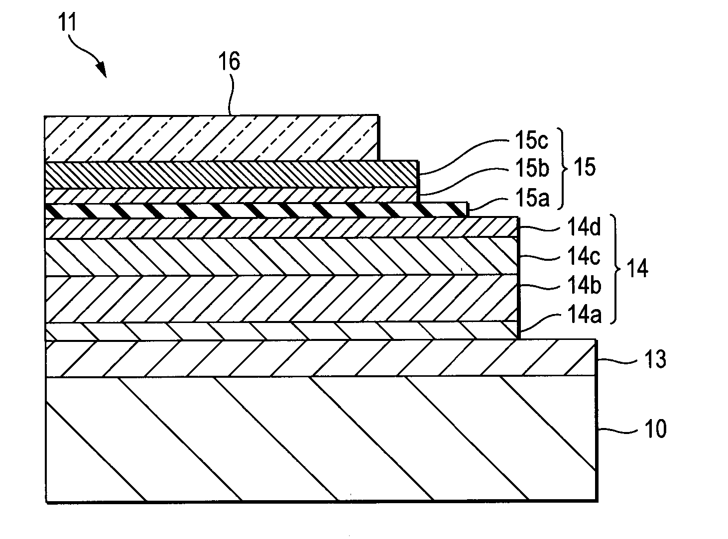
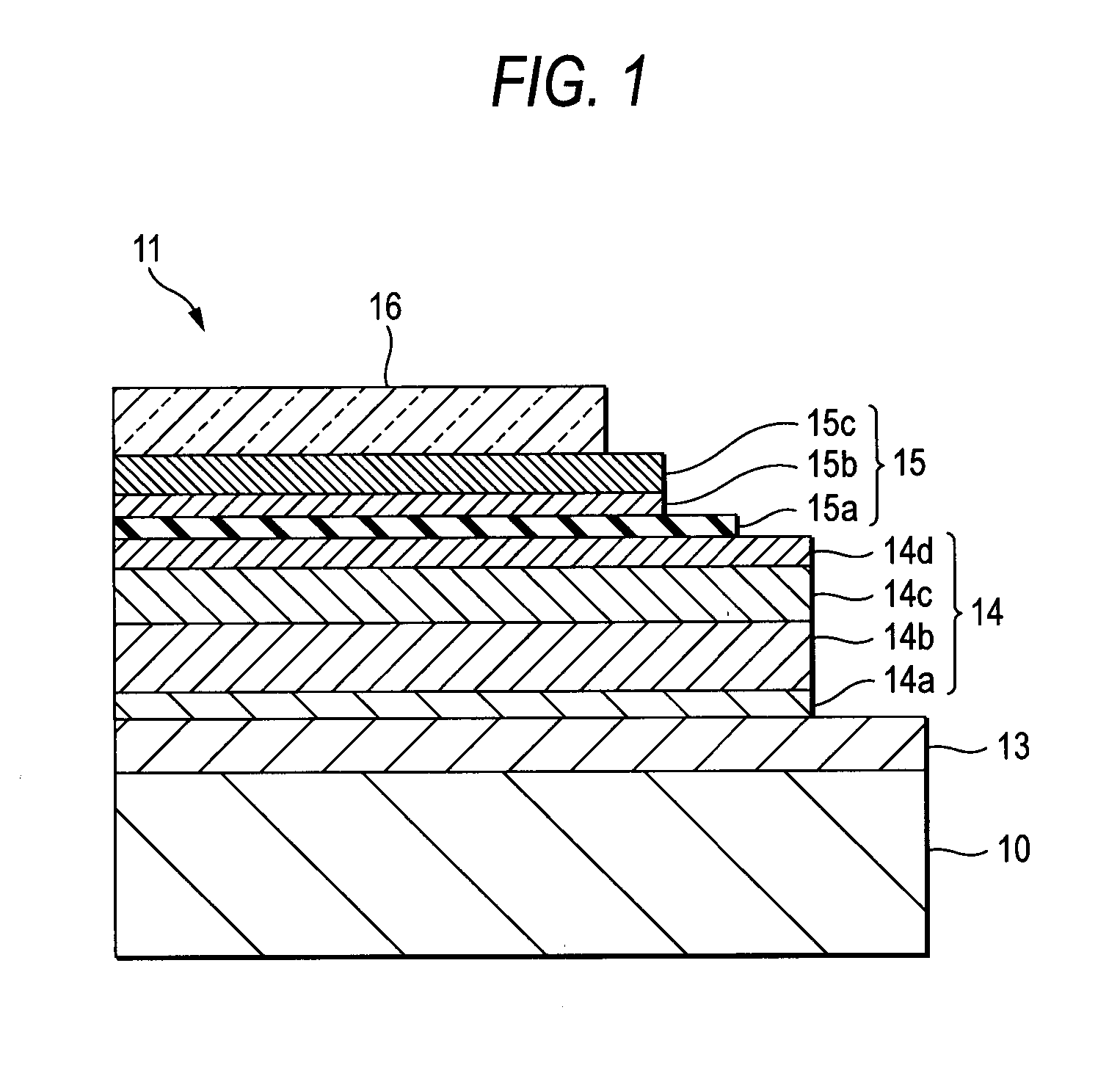
[0075] In this example, an organic electroluminescence device in which the electron injection layer 15 has a two-layered structure was manufactured.

[0076] At first, an Ag—Pd—Cu layer was formed on a substrate of a glass plate sized 30 mm×30 mm and an ITO layer was formed thereon to form a lower electrode 13 of a two-layered structure as an anode. Subsequently, a film of SiO2 was formed by sputtering and patterned by lithography to manufacture a cell for use in an organic electroluminescence device masked for a portion other than a 2 mm×2 mm light emission region with an insulative film (not illustrated).

[0077] Then, as the hole injection layer 14a, 2-TNATA (4,4≡,4≡-tris(2-naphtylphenylamino)triphenylaminel was vapor deposited at a film thickness of 15 nm (vapor deposition rate: 0.2 to 0.4 mm / sec).

[0078] Then, an α-NPD (α-naphthyl phenyl diamine) was formed by vapor deposition at film thickness of 15 nm (vapor deposition rate: 0.2 to 0.4 nm / sec) as the hole transporting layer.

[00...

example 2

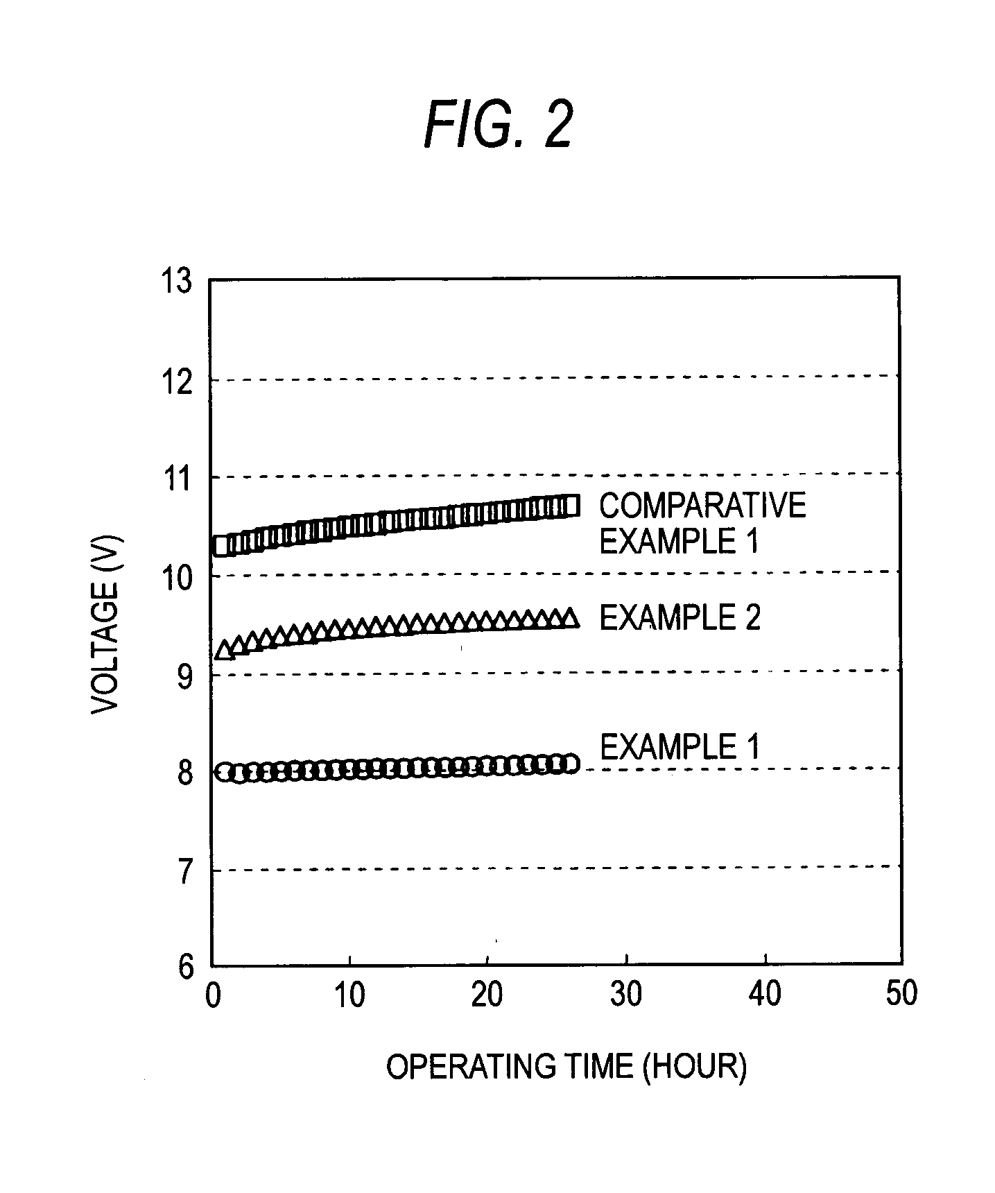
[0085] An organic electroluminescence device was manufactured in the same manufacturing procedures as those in Example 1 except for forming the protective layer 15c with an Mg—Ag alloy. In the formation of the protective layer 15c, the Mg—Ag alloy was co-vapor deposited to a film thickness of 2 nm at a weight ratio of Mg:Ag=100:5.

example 3

[0086] An organic electroluminescence device was manufactured in the same manufacturing procedures as those in Example 1 except for forming the protective layer 15c as the mixed layer comprising α-NP⊃ and Mg as the hole transporting material. In the formation of the protective layer 15c, the α-NPD-Mg alloy was co-vapor deposited at a film thickness of 5 nm at a weight ratio of α-NPD:Mg=100:5.


PUM


Abstract

An organic electroluminescence device including a lower electrode disposed on a substrate, an organic layer having at least a light emission layer and disposed above the lower electrode, and upper electrode having a transparent conductive film and disposed above the organic layer, in which the device has an electron injecting layer between the organic layer and the upper electrode. The electron injecting layer has a buffer layer comprising an insulative material and a mixed layer comprising an organic material that has an electron transporting property and a metal material that has an electron injecting property.

Description

CROSS REFERENCE TO RELATED APPLICATIONS [0001] The present invention contains subject matter related to Japanese Patent Application JP 2005-107036 filed on Apr. 4, 2005 and JP 2005-177215 filed on Jun. 17, 2005 in the Japanese Patent Office, the entire contents of which being incorporated herein by reference. BACKGROUND OF THE INVENTION [0002] 1. Field of the Invention [0003] The present invention concerns an organic electroluminescence device. [0004] 2. Description of the Related Art Organic electroluminescence devices are light emitting devices capable of operating at low voltage and suitable to saving of power consumption. Accordingly, they have now been used generally as light emitting devices for use in display devices and illumination devices. The organic electroluminescence device usually has a structure in which a lower electrode, an organic layer formed by laminating an organic hole transporting layer and an organic light emitting layer, and an upper electrode in this order...

Claims


Application Information

Patent Timeline
IPC IPC(8): H01J1/62H05B33/28H05B33/12
CPCH01L51/0059H01L51/0081H01L51/5092H01L51/5234H01L51/5278H01L51/5072H05B33/22H05B33/28Y10S428/917H01L27/3209H01L51/5056H01L2251/5315H10K85/631H10K85/324H10K50/171H10K50/828H10K50/19H10K2102/3026H10K59/32H10K50/15H10K50/16
Inventor SHIBANUMA, TETSUOMATSUDA, EISUKEKIJIMA, YASUNORINAKAMURA, HIROFUMIMATSUNAMI, SHIGEYUKI
Owner SONY CORP
Why Eureka
Try Eureka