Display device

a display device and display technology, applied in the direction of brake action initiation, instruments, vehicle components, etc., can solve the problems of increased manufacturing process and drawbacks of the cmos circuit, and achieve the effect of reducing the circuit scale and preventing the increase of the number of elements

Active Publication Date: 2006-10-05
JAPAN DISPLAY INC +1
View PDF3 Cites 15 Cited by
  • Summary
  • Abstract
  • Description
  • Claims
  • Application Information

AI Technical Summary

Benefits of technology

[0030] According to the present invention, it is possible to provide the display device which includes the common electrode drive circuit having the single chann

Problems solved by technology

However, the CMOS circuit has a drawback

Method used


Image

  • Display device
  • Display device
  • Display device

Examples


Embodiment Construction

[0051] Hereinafter, embodiments in which the present invention is applied to an active matrix-type liquid crystal display device are explained in detail in conjunction with drawings.

[0052] Here, in all drawings for explaining the embodiments, same symbols are given to parts having identical functions and their repeated explanation is committed.

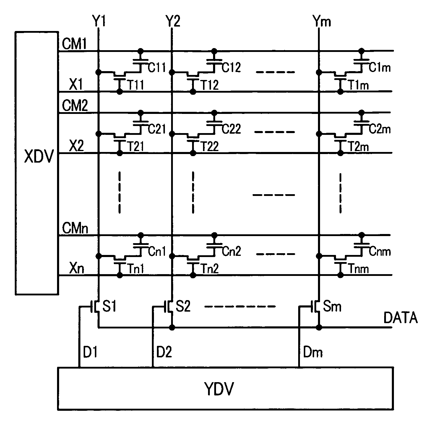
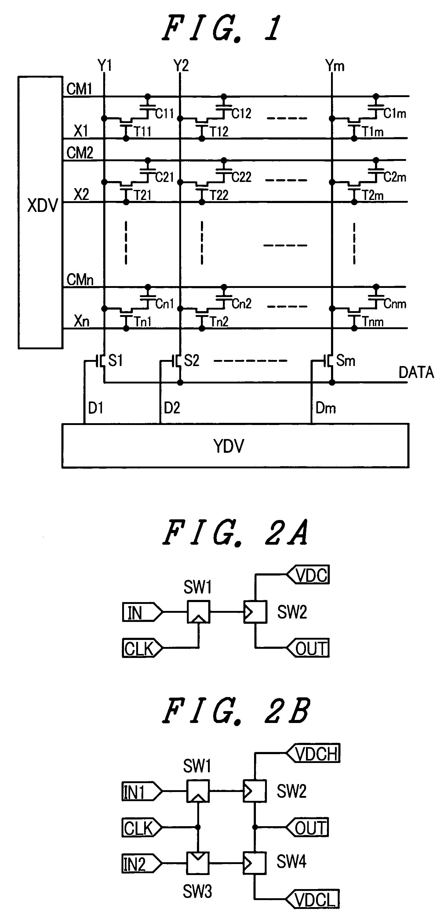
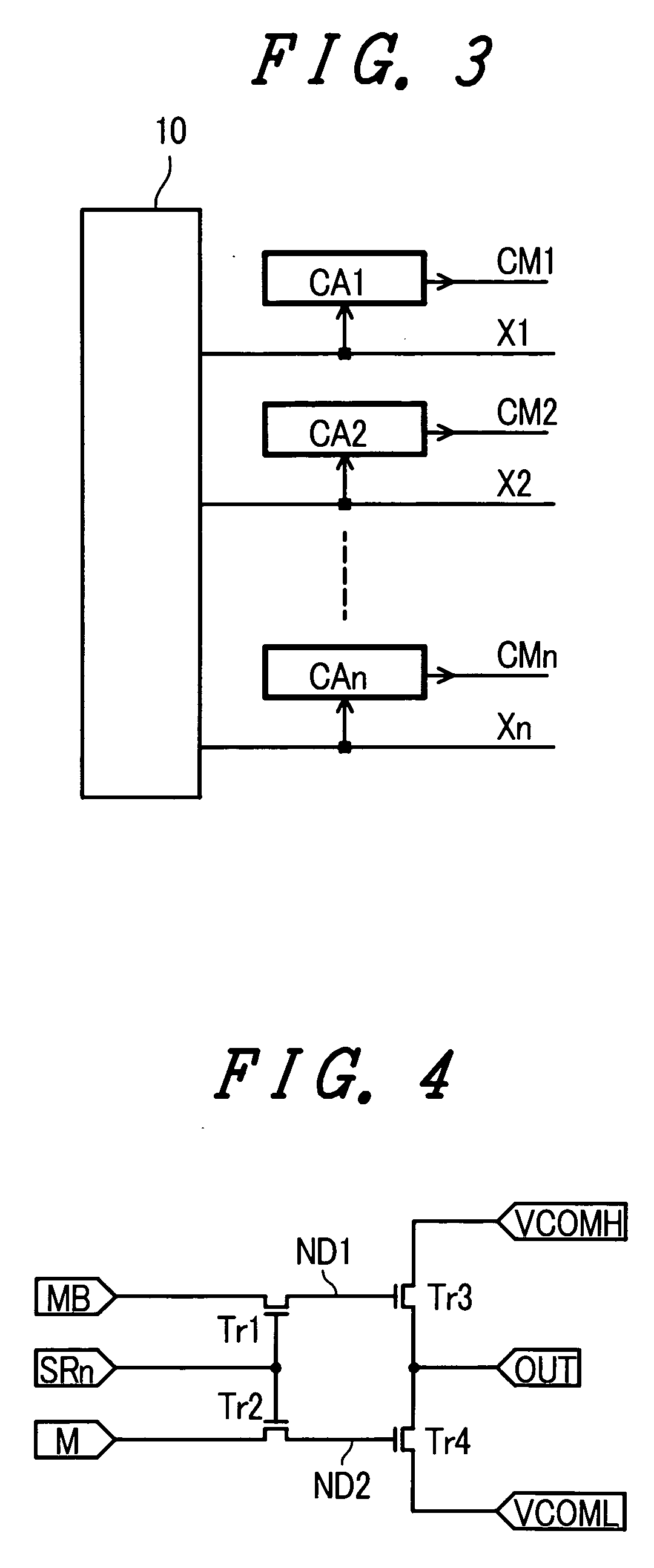
[0053]FIG. 1 is a circuit diagram showing an equivalent circuit of the active matrix type liquid crystal display device of the embodiment of the present invention.

[0054] As shown in FIG. 1, the active matrix type liquid crystal display device of this embodiment is an active matrix type liquid crystal display device which uses an IPS (In Plane Switching) liquid crystal display panel, wherein on a liquid crystal surface of one substrate out of a pair of substrates which are arranged to face each other with liquid crystal therebetween, n pieces of gate lines (X1, X2, . . . ,Xn) which extend in the x direction, n pieces of common lines (CM1, CM...


PUM


Abstract

The present invention provides a display device which includes a common electrode drive circuit having the single channel constitution which can miniaturize a circuit scale without increasing elements compared to a conventional display device. A display device includes a plurality of pixels and a common electrode drive circuit. The common electrode drive circuit includes a plurality of basic circuits, wherein the basic circuit includes a first circuit which latches a first input signal at a point of time that a clock signal is changed to a first voltage level from a second voltage level; a second circuit which latches a second input signal at the point of time that the clock signal is changed to the first voltage level from the second voltage level; a first switching circuit which is turned on based on the voltage latched by the first circuit and outputs a first power source voltage to an output terminal in an ON state; and a second switching circuit which is turned on based on the voltage which is latched by the second circuit and outputs a second power source voltage to an output terminal in an ON state, wherein when the first input signal assumes the second voltage level, the second input signal assumes the first voltage level, and when the second input signal assumes the second voltage level, the first input signal assumes the first voltage level, and after the clock signal is changed to the second voltage level from the first voltage level and before the clock signal returns to the first voltage level from the second voltage level, either one of the first input signal and the second input signal is changed to the second voltage level form the first voltage level.

Description

[0001] The present application claims priority from Japanese application JP2005-096624 filed on Mar. 30, 2005, the content of which is hereby incorporated by reference into this application. BACKGROUND OF THE INVENTION [0002] 1. Field of the Invention [0003] The present invention relates to a display device, and more particularly to a display device which includes a common electrode drive circuit adopting an every-line-independent common AC drive method. [0004] 2. Description of the Related Art [0005] A liquid crystal display module adopting a TFT (Thin Film Transistor) system has been popularly used as a display device of a portable equipment such as a notebook-type personal computer. Particularly, a liquid crystal display module which includes a miniaturized liquid crystal display panel is used as a display device of a portable equipment such as a mobile phone which a user always carries with him / her, for example. [0006] In general, when the same voltage (DC voltage) is applied to...

Claims


Application Information

Patent Timeline
IPC IPC(8): G09G3/36
CPCG09G3/3655B60T7/085B60Y2300/18141
Inventor NAKAO, TAKAYUKISATO, HIDEOMAKI, MASAHIROMIYAZAWA, TOSHIO
Owner JAPAN DISPLAY INC
Why Eureka
Try Eureka