Use of data latches in cache operations of non-volatile memories

a non-volatile memory and data latch technology, applied in the direction of memory architecture accessing/allocation, instruments, sustainable buildings, etc., can solve the problems of prone to mechanical failure, unsuitable mobile and handheld environment, and bulky disk drives

Active Publication Date: 2006-10-05
SANDISK TECH LLC
View PDF53 Cites 68 Cited by
  • Summary
  • Abstract
  • Description
  • Claims
  • Application Information

AI Technical Summary

Benefits of technology

[0048] An exemplary embodiment is based on a four state memory storing two-bits per cell and having two latches for data on each bit line and one additional latch for quick pass write. The operations of writing the lower page, or erasing, or doing a post erase soft program are basically a binary operation and have one of the data latches free, which can use it to cache data. Similarly, where doing an upper page or full sequence write, once all but the highest level has verified, only a single state needs to verify and the memory can free up a latch that can be used to cache data. An example of how this can be used is that when programming one page, such as in a copy operation, a read of another page that shares the same set of data latches, such as another word line on the same set of bit lines, can be slipped in between program pulse and verifies of the write. The address can then be switched to the page being written, allowing the write process to pick up where it left off without having to restart. While the write continues, the data cached during the interpolated read can be toggled out, checked or modified and transferred back to be present for writing back in once the earlier write operation completes. This sort cache operation allows the toggling out and modification of the second page of data to be hidden behind the programming of the first page.

Problems solved by technology

Conventional mass storage, based on rotating magnetic medium such as hard drives and floppy disks, is unsuitable for the mobile and handheld environment.
This is because disk drives tend to be bulky, are prone to mechanical failure and have high latency and high power requirements.
These undesirable attributes make disk-based storage impractical in most mobile and portable applications.
It is often difficult to perform both of these functions in an optimum manner with a single voltage.
Programming of charge storage memory devices can only result in adding more charge to its charge storage elements.
However, as can be seen from FIG. 6A, the circuitry of a read / write module will likely be implemented with many more transistors and circuit elements and therefore will occupy a space over many columns.
However, the interleaving page architecture is disadvantageous in at least three respects.
First, it requires additional multiplexing circuitry.
Secondly, it is slow in performance.
Thirdly, it is also not optimum in addressing other disturb effects such as field coupling between neighboring charge storage elements at the floating gate level when the two neighbors are programmed at different times, such as separately in odd and even pages.
The problem of neighboring field coupling becomes more pronounced with ever closer spacing between memory transistors.
The conventional architecture of interleaving page exacerbates the error caused by neighboring floating gate coupling.
The read errors will become more severe with increasing density, requiring a more accurate read operation and coarser partitioning of the threshold window for multi-state implementation.
Performance will suffer and the potential capacity in a multi-state implementation is limited.

Method used


Image

  • Use of data latches in cache operations of non-volatile memories
  • Use of data latches in cache operations of non-volatile memories
  • Use of data latches in cache operations of non-volatile memories

Examples


Embodiment Construction

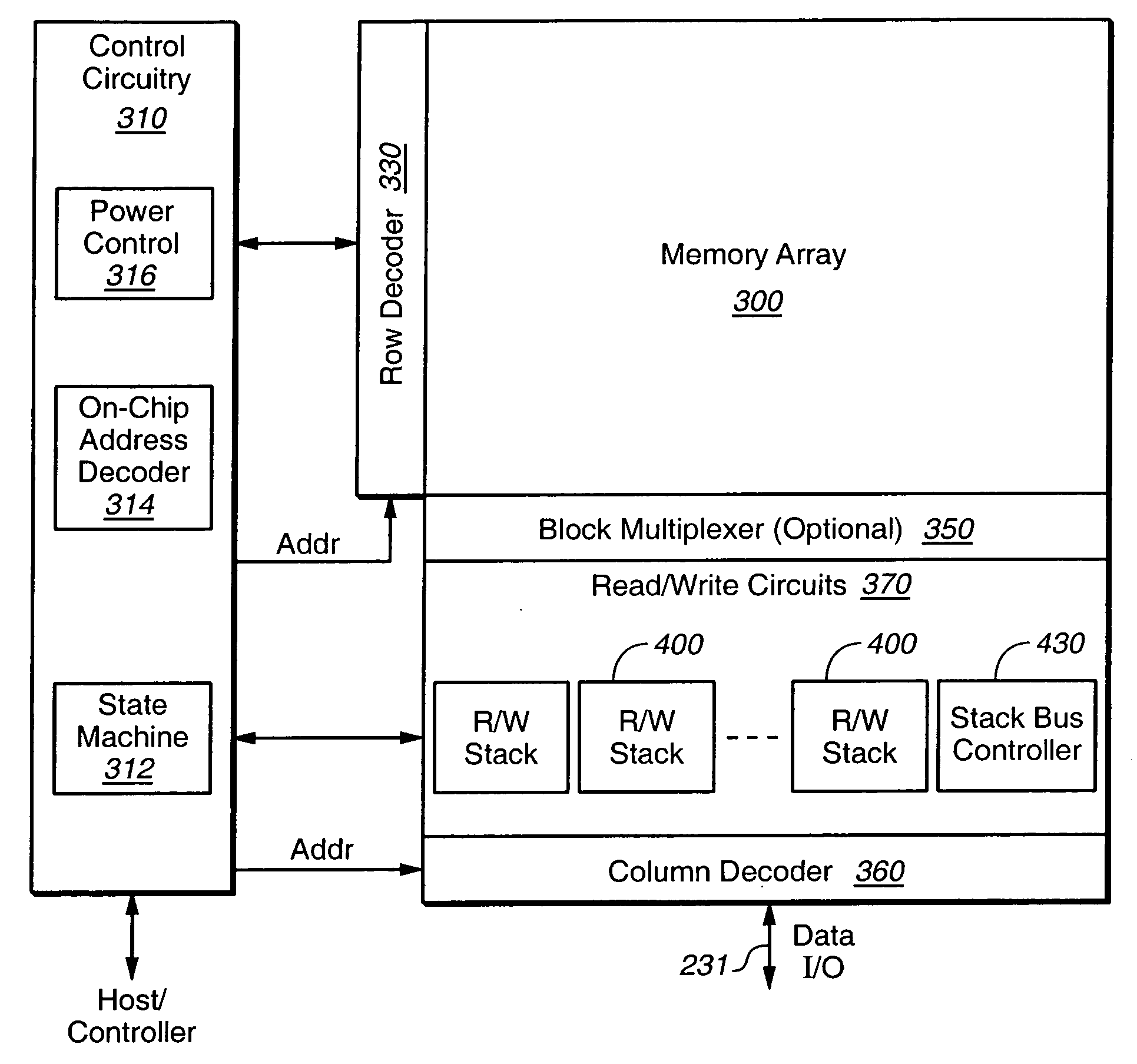
[0073]FIG. 7A illustrates schematically a compact memory device having a bank of partitioned read / write stacks, in which the improved processor of the present invention is implemented. The memory device includes a two-dimensional array of memory cells 300, control circuitry 310, and read / write circuits 370. The memory array 300 is addressable by word lines via a row decoder 330 and by bit lines via a column decoder 360. The read / write circuits 370 is implemented as a bank of partitioned read / write stacks 400 and allows a block (also referred to as a “page”) of memory cells to be read or programmed in parallel. In a preferred embodiment, a page is constituted from a contiguous row of memory cells. In another embodiment, where a row of memory cells are partitioned into multiple blocks or pages, a block multiplexer 350 is provided to multiplex the read / write circuits 370 to the individual blocks.

[0074] The control circuitry 310 cooperates with the read / write circuits 370 to perform me...


PUM


Abstract

Methods and circuitry are present for improving performance in non-volatile memory devices by allowing the inter-phase pipelining of operations with the same memory, allowing, for example, a read operation to be interleaved between the pulse and verify phases of a write operation. In the exemplary embodiment, the two operations share data latches. In specific examples, at the data latches needed for verification in a multi-level write operation free up, they can be used to store data read from another location during a read performed between steps in the multi-level write. In the exemplary embodiment, the multi-level write need only pause, execute the read, and resume the write at the point where it paused.

Description

CROSS REFERENCE TO RELATED APPLICATIONS [0001] This application is related to the following U.S. patent applications: Ser. No. 11 / 013,125, filed Dec. 14, 2004; Ser. No. 11 / 026,536, filed Dec. 29, 2004; Ser. No. 11 / 015,199, filed Dec. 16, 2004; a patent application entitled “Non-Volatile Memory and Method with Power-Saving Read and Program-Verify Operations”, by Yan Li, Seungpil Lee, and Siu Lung Chan, filed Mar. 16, 2005; and a patent application entitled “Use of Data Latches in Multi-Phase Programming of Non-Volatile Memories”, by Yan Li and Raul-Adrian Cernea, filed concurrently with the present application. These applications are incorporated herein by reference in their entirety for all purposes.FIELD OF THE INVENTION [0002] This invention relates generally to non-volatile semiconductor memory such as electrically erasable programmable read-only memory (EEPROM) and flash EEPROM, and specifically to cache operations based on shared latch structures allowing overlapping memory ope...

Claims


Application Information

Patent Timeline
Patent Type & Authority Applications(United States)
IPC IPC(8): G11C16/04
CPCG06F12/0893G06F2212/2022G06F2212/3042Y02B60/1225G11C16/26G11C2207/2245G11C16/04G11C7/22Y02D10/00G11C16/06G11C16/10G11C16/34
Inventor LI, YANYERO, EMILIO
Owner SANDISK TECH LLC
Why Eureka
Try Eureka