Use of deep-level transitions in semiconductor devices

a technology of semiconductor devices and transitions, applied in the direction of semiconductor devices, basic electric elements, electrical equipment, etc., can solve the problems of insufficient integration of inp circuits, high cost, and inability to actually put together parts of optical modules, and achieve the effect of “engineering” of useful devices

Inactive Publication Date: 2006-10-12
YALE UNIV
View PDF4 Cites 4 Cited by
  • Summary
  • Abstract
  • Description
  • Claims
  • Application Information

AI Technical Summary

Benefits of technology

[0014] In general terms, the invention relates to the design, fabrication, and use of semiconductor devices that employ deep-level transitions (i.e., deep-level-to-conduction-band, deep-level-to-valence-band, or deep-level-to-deep-level) to achieve useful results. To facilitate the

Problems solved by technology

However, InP circuits have not achieved a level of device integration which is anywhere near that of GaAs device integration.
At present, the lack of very large scale monolithic integration of InP circuits with InGaAs optical devices has meant t

Method used


Image

  • Use of deep-level transitions in semiconductor devices
  • Use of deep-level transitions in semiconductor devices
  • Use of deep-level transitions in semiconductor devices

Examples


Embodiment Construction

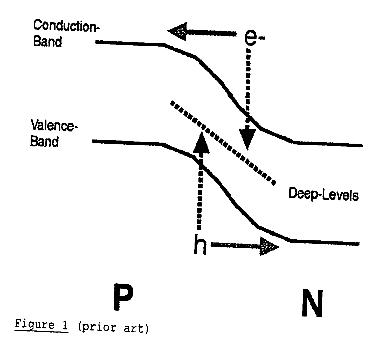
[0043] Conventional behavior is illustrated in FIG. 1. In a conventional p-n junction, electron transport occurs through the conduction band, and hole transport occurs through the valence band. (This transport through a conventional p-n junction is indicated by the solid arrows.) In a conventional p-n junction, deep-levels act as nonradiative recombination centers. (This is indicated by the dotted arrows, which show the trapping by deep-levels of electrons from the conduction band and holes from the valence band.)

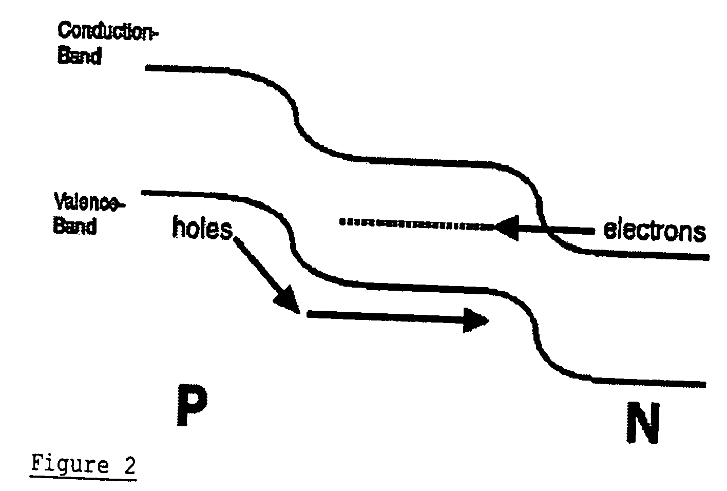
[0044]FIG. 2 shows a band diagram for an exemplary deep-level optical emitter. In this device, an optical transition occurs between the deep-level (indicated by the dashed line) and the valence-band. Electrons are injected into the deep-level from the n-type region, whereas holes are injected from the p-type region into the optically-active central region.

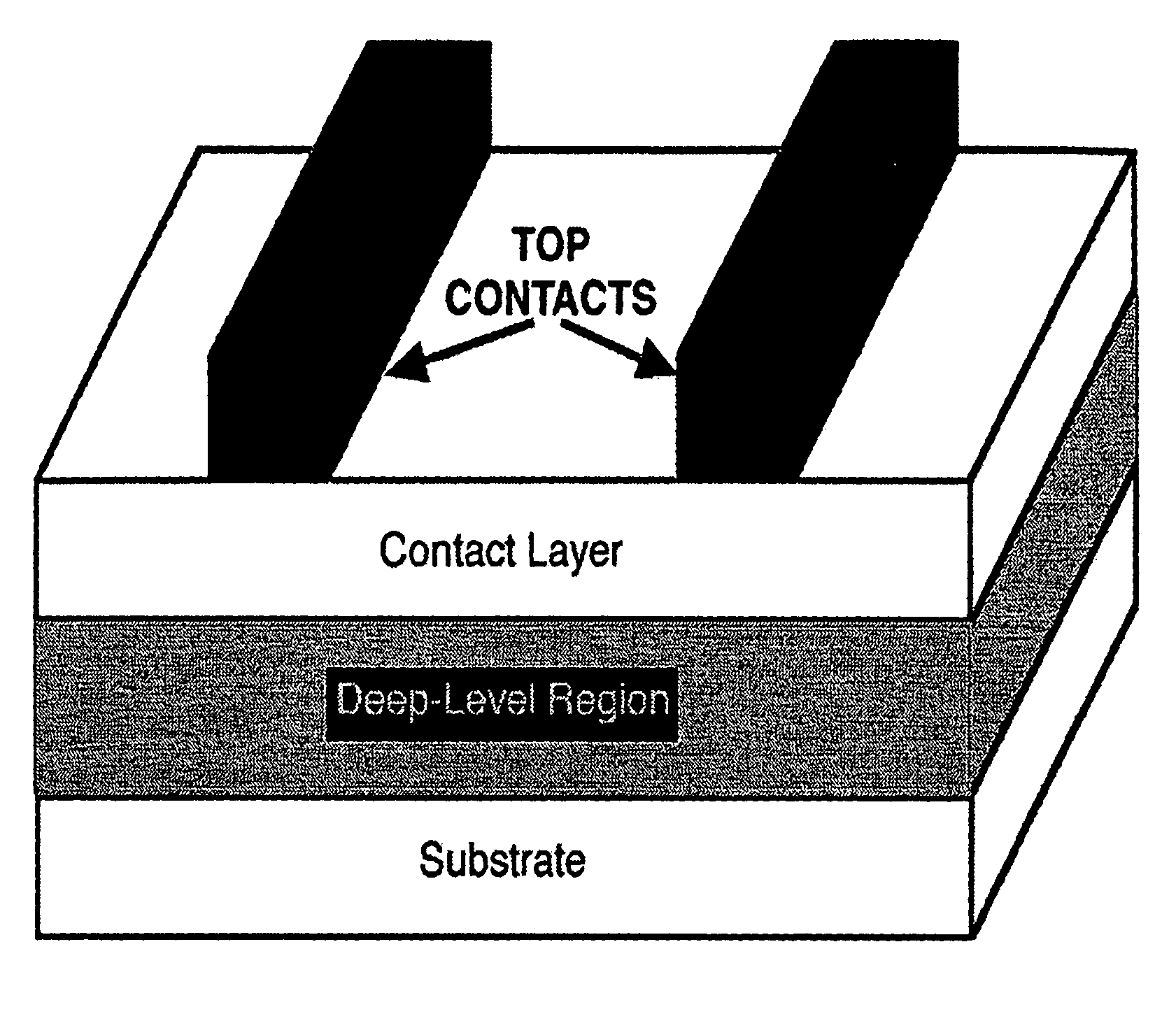
[0045] In FIG. 3, the efficiency of the deep-level optical emitter is improved through the addition of a Schottky cont...


PUM


Abstract

The invention relates to the design, fabrication, and use of semiconductor devices that employ deep-level transitions (i.e., deep-level-to-conduction-band, deep-level-to-valence-band, or deep-level-to-deep-level) to achieve useful results. A principal aspect of the invention involves devices in which electrical transport occurs through a band of deep-level states and just the conduction band (or through a deep-level band and just the valence band), but where significant current does not flow through all three bands. This means that the deep-state is not acting as a nonradiative trap, but rather as an energy band through which transport takes place. Advantageously, the deep-level energy-band may facilitate a radiative transition, acting as either the upper or lower state of an optical transition.

Description

CROSS-REFERENCE TO RELATED APPLICATIONS [0001] This application claims priority from U.S. Provisional Patent Applications Ser. No. 60 / 408,488 (filed Sep. 4, 2002) and Ser. No. 60 / 420,886 (filed Oct. 24, 2002), both of which are incorporated herein by reference.FIELD OF THE INVENTION [0002] The present invention relates generally to the field of semiconductor materials and devices, and more specifically to semiconductor materials and devices having an “artificial” energy band comprised of deep-level states. BACKGROUND OF THE INVENTION [0003] All semiconductor materials are characterized by an energy gap (EG) greater than zero. The energy gap is defined as the difference between the conduction-band edge (EC) and the valence-band edge (EV). A deep-level state is defined as a state having an energy level at least 0.05 EG above the valence-band edge and at least 0.05 EG below the conduction-band edge. [0004] A deep-level state can arise from a bound state of a substitutional impurity, an...

Claims


Application Information

Patent Timeline
IPC IPC(8): H01L31/00
CPCH01L31/03042Y02E10/544H01L33/0041
Inventor PAN, JANET L.
Owner YALE UNIV
Why Eureka
Try Eureka