Method and apparatus for controlling a voltage level

a voltage level and voltage technology, applied in the field of data processing, can solve problems such as the introduction of a new problem of data loss, and achieve the effect of convenient and efficient switching devices

Active Publication Date: 2006-10-12
ARM LTD
View PDF6 Cites 17 Cited by
  • Summary
  • Abstract
  • Description
  • Claims
  • Application Information

AI Technical Summary

Benefits of technology

[0010] The introduction of power transistors that allow a circuit to be put into a sleep mode has reduced the problem of static power loss but has introduced a new problem of data loss. The voltage level control device of the present invention recognises the conflicting problems of power loss and data loss and addresses these problems in a simple and elegant fashion by providing at least one additional switching device in parallel with the power transistor, the switching device(s) being provided with their own sleep input(s). The provision of this additional switching device(s) with additional control input means that at least three different voltage levels can be output by the voltage level control device. Thus, the potential difference across circuitry can be set by this device to be one of at least three values, the largest potential difference being chosen for active mode, the lowest potential difference being chosen for sleep mode, and additional intermediate potential difference(s) being provided which can be used for “pseudo sleep” mode(s). In pseudo sleep mode the voltage across the circuit is reduced thus, power loss is reduced. However there is still a sufficient voltage across the circuit to avoid or at least reduce data loss. This mode can be particularly useful for situations where circuitry is inactive for a short period.
[0012] By having the first and second voltage levels substantially equal to the voltage level of the voltage sources the voltage differences approaching the maximum and minimum possible can be achieved across the circuitry. These are appropriate for active and sleep mode respectively. At least one intermediate voltage level can be used and this is selected to be an appropriate level for reducing data loss while increasing power savings.
[0014] A sleep signals act to turn off the power transistor. Providing a switching device in parallel to the power transistor with a separate input for a pseudo sleep signal enables three different voltage levels to be output, depending on the values of the two sleep signals. This enables a sleep mode where power loss is very low but data is not retained, a pseudo sleep mode sufficient to retain at least some data while reducing power loss compared to an active mode where power loss may be relatively high and state is retained.
[0018] NMOS transistors are particularly suitable for power transistors and are often used, having a low area and low resistance.
[0020] A PMOS transistor is suitable for use as a switch in conjunction with an NMOS transistor. A PMOS transistor forms a relatively small switching device and is also quite cheap to manufacture. Furthermore the threshold voltage of the PMOS transistor can (within limits) be selected by using appropriate VT masks. Thus, a suitable intermediate voltage that reduces power loss while ensuring data retention can be selected.
[0024] An NMOS transistor placed in parallel with a PMOS power transistor makes a convenient and efficient switching device.

Problems solved by technology

The introduction of power transistors that allow a circuit to be put into a sleep mode has reduced the problem of static power loss but has introduced a new problem of data loss.

Method used


Image

  • Method and apparatus for controlling a voltage level
  • Method and apparatus for controlling a voltage level
  • Method and apparatus for controlling a voltage level

Examples


Embodiment Construction

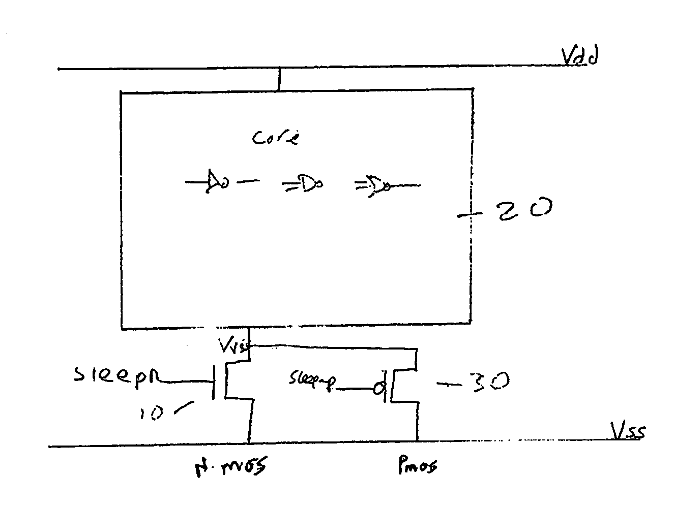
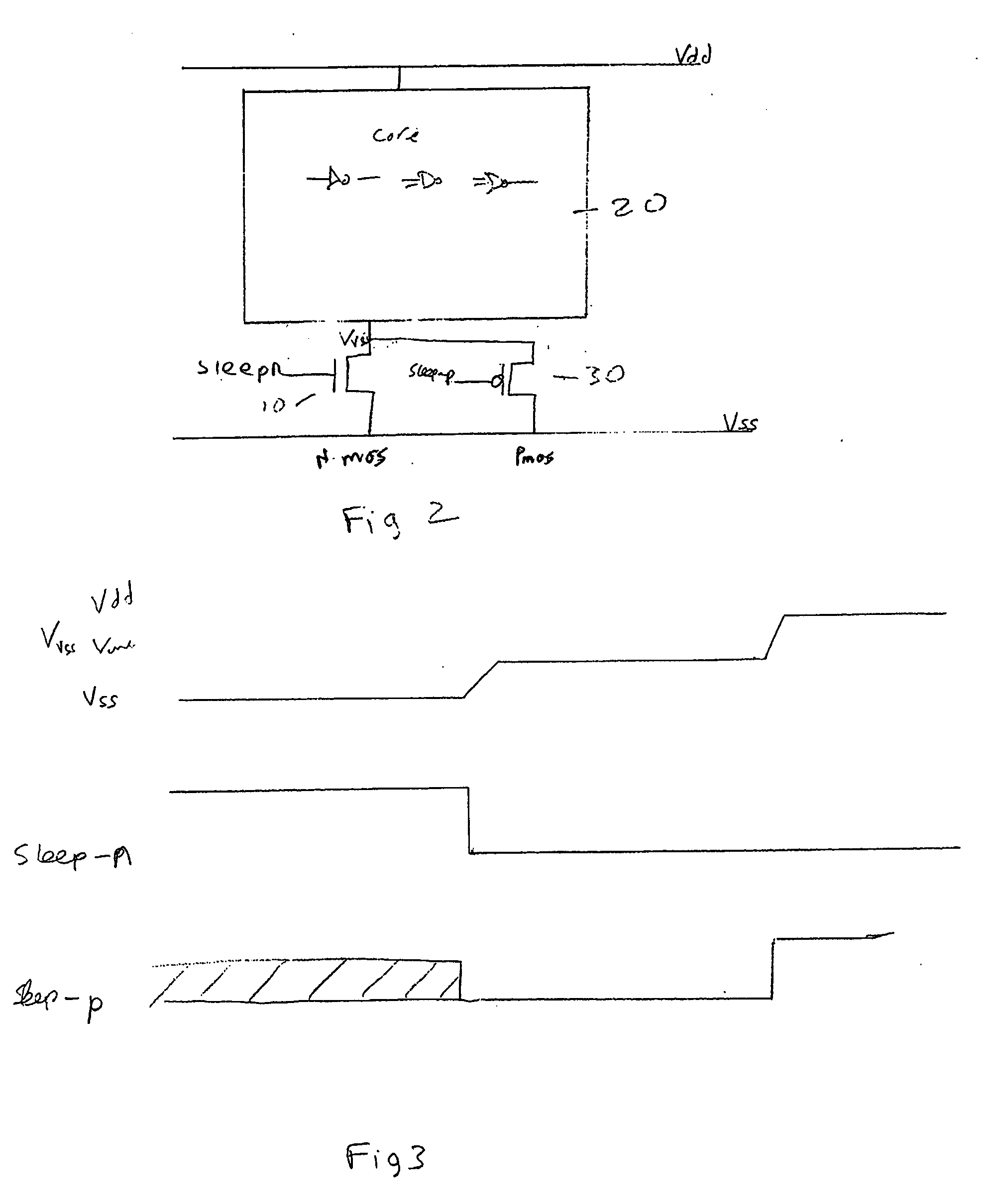
[0042]FIG. 2 schematically shows a core of logic 20, which may comprise data storage elements, data processing elements and / or circuitry in general, powered by a high voltage rail Vdd and a low voltage rail Vss. The low voltage rail is generally held at ground. An NMOS power transistor 10 is connected between the core logic 20 and the lower voltage rails Vss. This NMOS power transistor 10 receives a sleep signal sleepn at its gate. When the sleepn signal is high, NMOS power transistor 10 is turned on and the voltage Vvss at its drain is approximately that of the lower voltage rail Vss i.e. it gives a virtual Vss to core logic 20. Thus, a high sleepn signal is in effect a no sleep signal and renders core logic 20 active. In this state, core logic 20 receives most of the voltage drop from between voltage rails Vdd and Vss, the voltage drop lost being that due to the voltage drop across the transistor due to its resistance when its on. This is designed to be small.

[0043] The voltage c...


PUM


Abstract

A voltage level control device operable to control a voltage level supplied from a first voltage level source to circuitry; said circuitry being arranged between said first voltage level source and a second voltage level source, said first and second voltage level sources being operable to output different voltage levels; said voltage level control device comprising: a power transistor operable to be connected between said first voltage level source and said circuitry, said power transistor comprising a sleep signal input operable to receive a sleep signal; a switching device arranged in parallel with said power transistor and comprising a sleep signal input operable to receive a pseudo sleep signal; wherein said voltage level control device is operable in dependence upon said sleep signal and said pseudo sleep signal to output to said circuitry an output voltage said output voltage comprising one of three voltage levels, said three voltage levels lying between voltage levels output by said first and second voltage sources.

Description

BACKGROUND OF THE INVENTION [0001] 1. Field of the Invention [0002] The present invention relates to the field of data processing and in certain preferred embodiments to the field of voltage level control. [0003] 2. Description of the Prior Art [0004] Many data processing circuits burn power even when they are not doing anything, this is referred to as static power leakage. Static power leakage is a particular problem in circuits where the components are manufactured to be as small as possible. To reduce power leakage, many circuit designs are now making use of power gating which helps reduce power leakage during sleep mode. This power gating is achieved by inserting power transistors between any circuit element and Vdd creating a “virtual” Vdd rail, or by inserting power transistors between any circuit element and Vss creating a “virtual” Vss rail. These transistors are placed in series with the circuit either between the high voltage rail Vdd and the circuit or between the low vol...

Claims


Application Information

Patent Timeline
Patent Type & Authority Applications(United States)
IPC IPC(8): H03K19/003
CPCH03K19/0016
Inventor CHONG, YEW KEONG
Owner ARM LTD
Why Eureka
Try Eureka