

Edge temperature compensation in thermal processing particularly useful for SOI wafers
a thermal processing and edge temperature compensation technology, applied in the field of thermal processing of semiconductor substrates and chambers, can solve the problems of crystallographic line defects, chips containing slip defects that are either inoperative or subject to early failure, and achieve the effect of less vertical structure and improving processing uniformity over tim
- Summary
- Abstract
- Description
- Claims
- Application Information
AI Technical Summary
Benefits of technology
Problems solved by technology
Method used
Image

Examples
Embodiment Construction
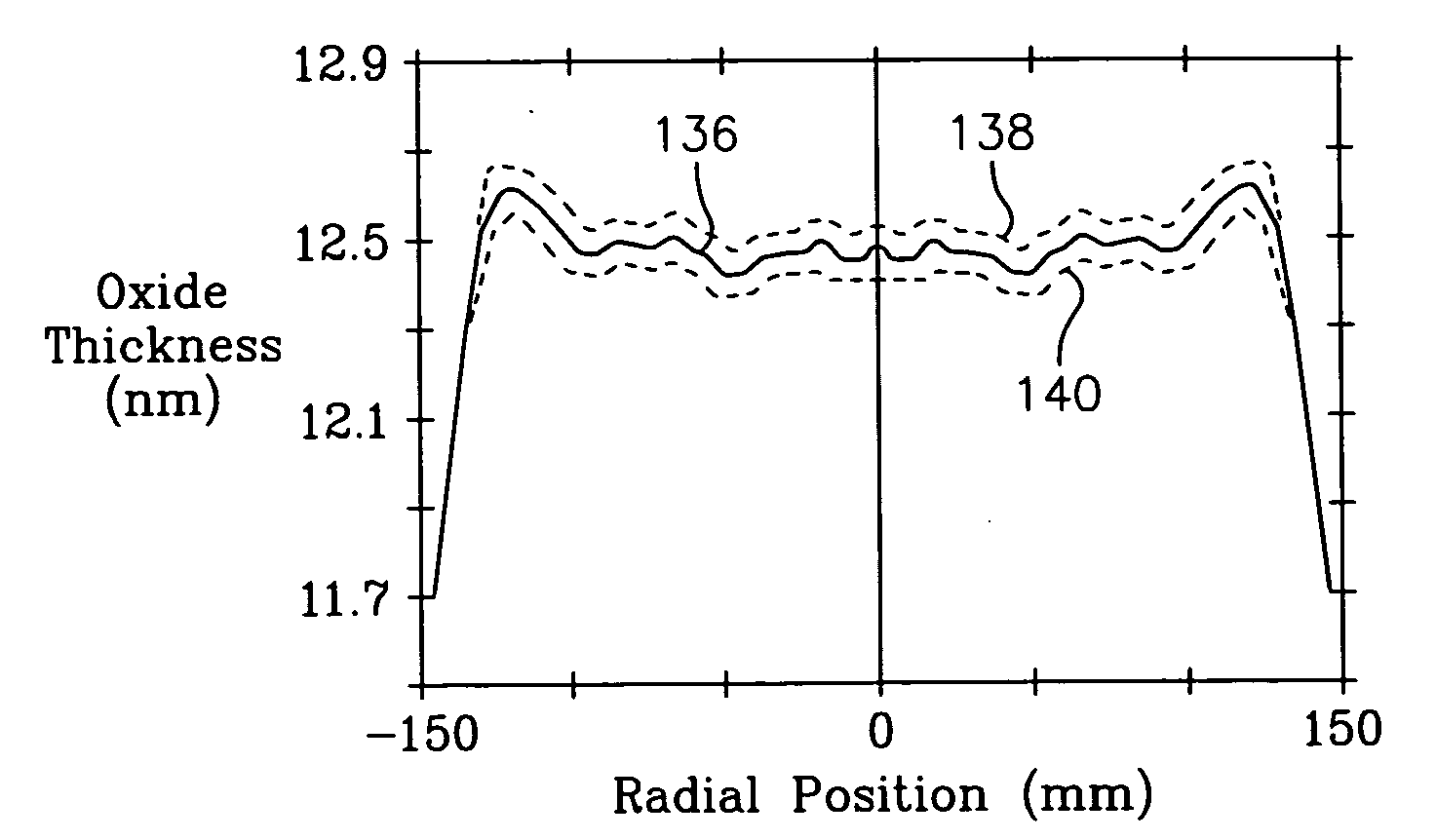
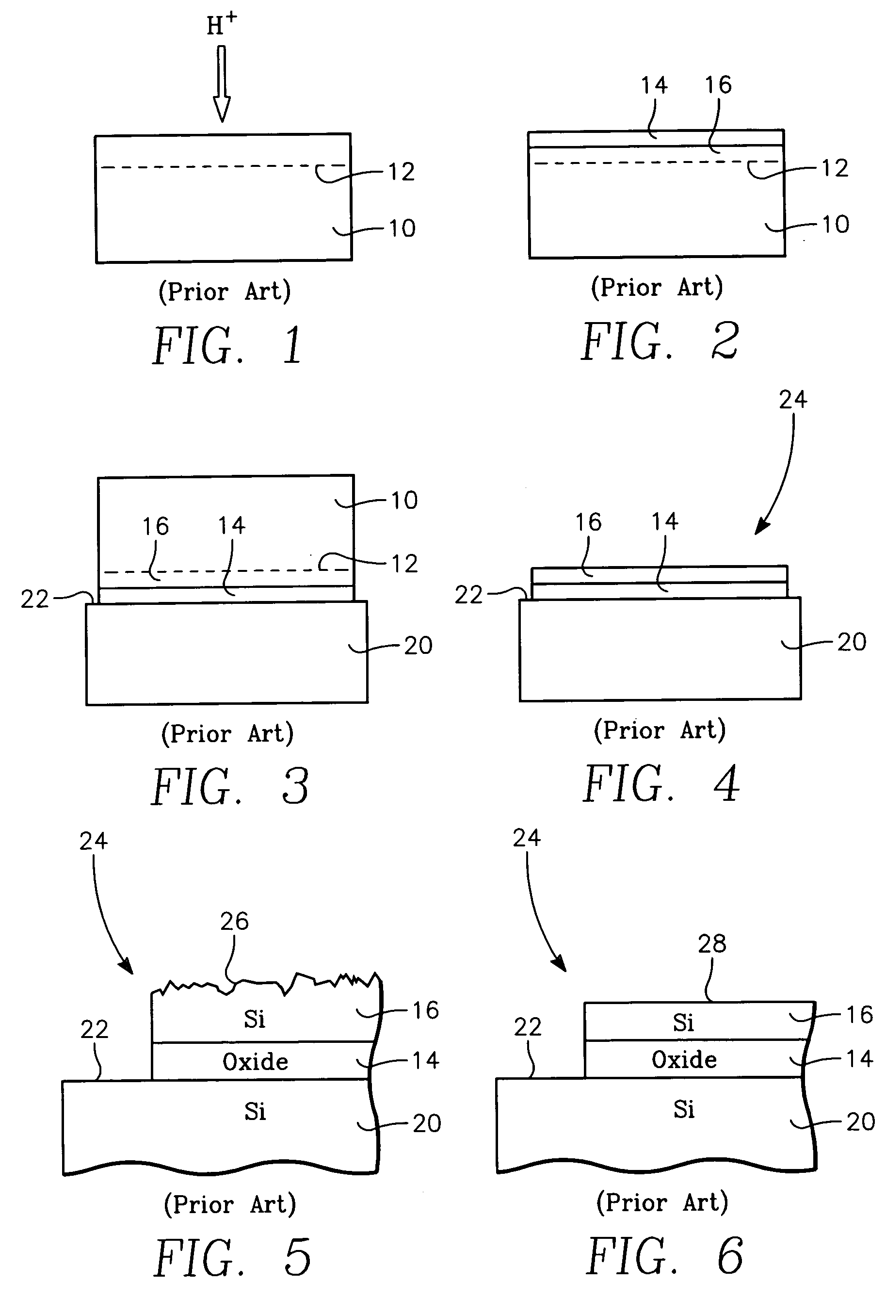
[0023] Although the invention is not limited by our understanding of its operation, we believe that the slip problem, particularly in semiconductor-on-insulator (SOI) wafers, in large part arises from the difference in emissivity between the narrow edge exclusion and the rest of the SOI wafer.
[0024] Before the apparatus and processes related to this invention are presented, it is important to understand a few of the principles that affect these types of processes. Three important material properties play a role in the way in body reacts when heated by optical radiation. These properties are:
[0025] 1. Absorptivity (α): For an object that is receiving heat by radiation, absorptivity is defined as the fraction of that total energy that is absorbed by it. For the same amount of heat radiation, an object with higher α will experience a faster temperature rise than one with lower absorptivity. If substantially all the radiation is absorbed in the object, then the differential temperatur...
PUM
 Abstract
Description
Claims
Application Information