Method of forming fine pitch photoresist patterns using double patterning technique

a patterning technique and patterning technology, applied in the field of photoresist pattern formation, can solve the problems of intermixing problem, insufficient resolution of krf or arf lasers,

Inactive Publication Date: 2006-10-12
SAMSUNG ELECTRONICS CO LTD
View PDF4 Cites 86 Cited by
  • Summary
  • Abstract
  • Description
  • Claims
  • Application Information

AI Technical Summary

Benefits of technology

[0014] Embodiments of the present invention provide methods of forming fine pitch photoresist patterns without the deformations that can result from the intermixing problem.

Problems solved by technology

Unfortunately, the resolution of these KrF or ArF lasers is not high enough to produce the fine pitch patterns required to form 1 GB DRAM devices.
One shortcoming of the conventional double patterning method is known as an intermixing problem.

Method used


Image

  • Method of forming fine pitch photoresist patterns using double patterning technique
  • Method of forming fine pitch photoresist patterns using double patterning technique
  • Method of forming fine pitch photoresist patterns using double patterning technique

Examples


Embodiment Construction

[0025] Exemplary embodiments of the invention are described below with reference to the corresponding drawings. These embodiments are presented as teaching examples. The actual scope of the invention is defined by the claims that follow.

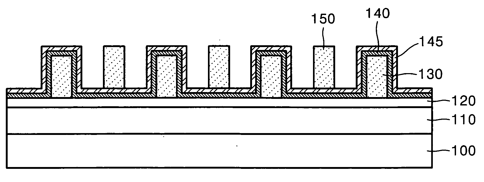
[0026]FIGS. 3A through 3C are cross-sectional views illustrating a method of forming fine pitch photoresist patterns using a double patterning method according to an embodiment of the present invention.

[0027] Referring to FIG. 3A, a layer 110 is formed on a semiconductor substrate 100. A bottom anti reflective coating (BARC) film 120 is then formed on layer 110. BARC film 120 comprises an organic material and is used to prevent diffused reflection in an exposure process used to form a first photoresist pattern 130. A first photoresist film (not shown) is formed on BARC film 120 and then first photoresist pattern 130 is formed by exposing and developing a portion of the first photoresist film. Preferably, first photoresist pattern 130 is formed to h...


PUM


Abstract

A method of forming a photoresist pattern comprises providing a semiconductor substrate on which a layer to be etched is formed. The method further comprises forming a first photoresist pattern on the layer to be etched, processing the first photoresist pattern with hydrogen bromide (HBr) plasma, and forming a second photoresist pattern on the semiconductor substrate between the first photoresist patterns

Description

BACKGROUND OF THE INVENTION [0001] 1. Field of the Invention [0002] Embodiments of the present invention relate generally to methods of forming photoresist patterns. More particularly, embodiments of the invention relate to methods of forming fine pitch photoresist patterns using a double patterning technique. [0003] A claim of priority is made to Korean Patent Application No. 10-2005-0028533, filed on Apr. 6, 2005, the disclosure of which is hereby incorporated by reference in its entirety. [0004] 2. Description of Related Art [0005] Researchers are continually searching for new ways to increase the performance of semiconductor devices such as computer memories and microprocessors. One of the main focuses of their research is developing techniques for fitting more electronic features such as transistors onto a small area of a wafer or substrate. In other words, the researchers seek to increase the performance of the semiconductor devices by increasing their integration density. [00...

Claims


Application Information

Patent Timeline
Patent Type & Authority Applications(United States)
IPC IPC(8): H01L21/302H01L21/461
CPCG03F7/0035G03F7/405H01L21/312H01L21/31138H01L21/0273H01L21/02167H01L21/02282H01L21/02304F21V23/026F21V29/508F21V29/74H05B41/02
Inventor CHAE, YUN-SOOKMIN, GYUNG-JINSHIN, CHUL-HOKIM, SANG-WOOK
Owner SAMSUNG ELECTRONICS CO LTD
Why Eureka
Try Eureka