Semiconductor device manufacturing method

a technology of semiconductor devices and manufacturing methods, applied in the direction of basic electric elements, electrical equipment, electric discharge tubes, etc., can solve the problems of mask shape not being maintained, and achieve the effects of small width, high verticality, and increased width of the shape at the bottom

Active Publication Date: 2015-02-05
TOKYO ELECTRON LTD
View PDF0 Cites 14 Cited by
  • Summary
  • Abstract
  • Description
  • Claims
  • Application Information

AI Technical Summary

Benefits of technology

[0011]In the step (b), a temperature of the target object in a first period may be set to be higher than a temperature of the target object in a second period following the first period. In other words, the temperature of the target object in the first period of the step (b) may be set to a relatively high level, and the temperature of the target objet in the second period of the step (b) may be set to a relatively low level. With such, it is possible to form, in the first period, a shape having a width that becomes gradually smaller toward the bottom in the depth direction and also possible to form a thick protective film on a surface defining the shape. Further, the width of the shape at the bottom can be increased in the second period. Accordingly, it is possible to form a shape, e.g., a hole, having a small width and a high verticality.
[0012]Alternatively, in the step (b), a temperature of the target object in the first period may be set to be lower than a temperature of the target object in the second period following the first period. In other words, the temperature of the target object may be set to a relatively low level in the first period of the step (b), and the temperature of the target object may be set to a relatively high level in the second period of the step (b). Accordingly, a high etching rate can be ensured in the first period, and a shape, e.g., a hole, with a small width, can be formed in the second period.
[0013]As described above, in accordance with the aspect of the present invention, a mask selectivity can be improved in etching for forming a shape with a large depth in the multilayer film.

Problems solved by technology

However, the shape of the mask may not be maintained against the plasma of the processing gas disclosed in U.S. Patent Application Publication No. 2013 / 0059450.

Method used


Image

  • Semiconductor device manufacturing method
  • Semiconductor device manufacturing method
  • Semiconductor device manufacturing method

Examples


Embodiment Construction

[0022]Hereinafter, embodiments of the present invention will be described with reference to the accompanying drawings. Meanwhile, like reference numerals will be used for like or corresponding parts in all the drawings.

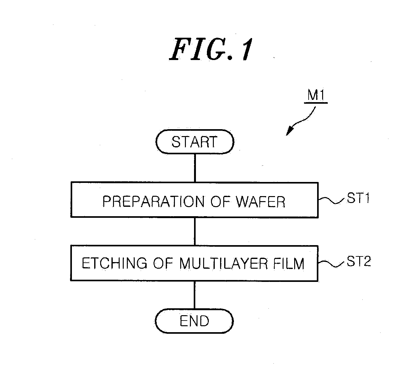
[0023]FIG. 1 is a flowchart showing a semiconductor device manufacturing method in accordance with an embodiment of the present invention. The semiconductor device manufacturing method MT shown in FIG. 1 includes steps ST1 and ST2 and may be used for manufacturing a NAND flash memory having a 3D structure, for example. In the step ST1, a target objet (hereinafter, referred to as “wafer”) W is prepared. In the step ST2, a multilayer film of the wafer W is etched.

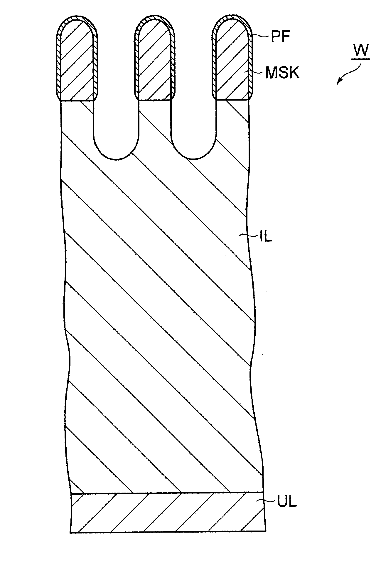
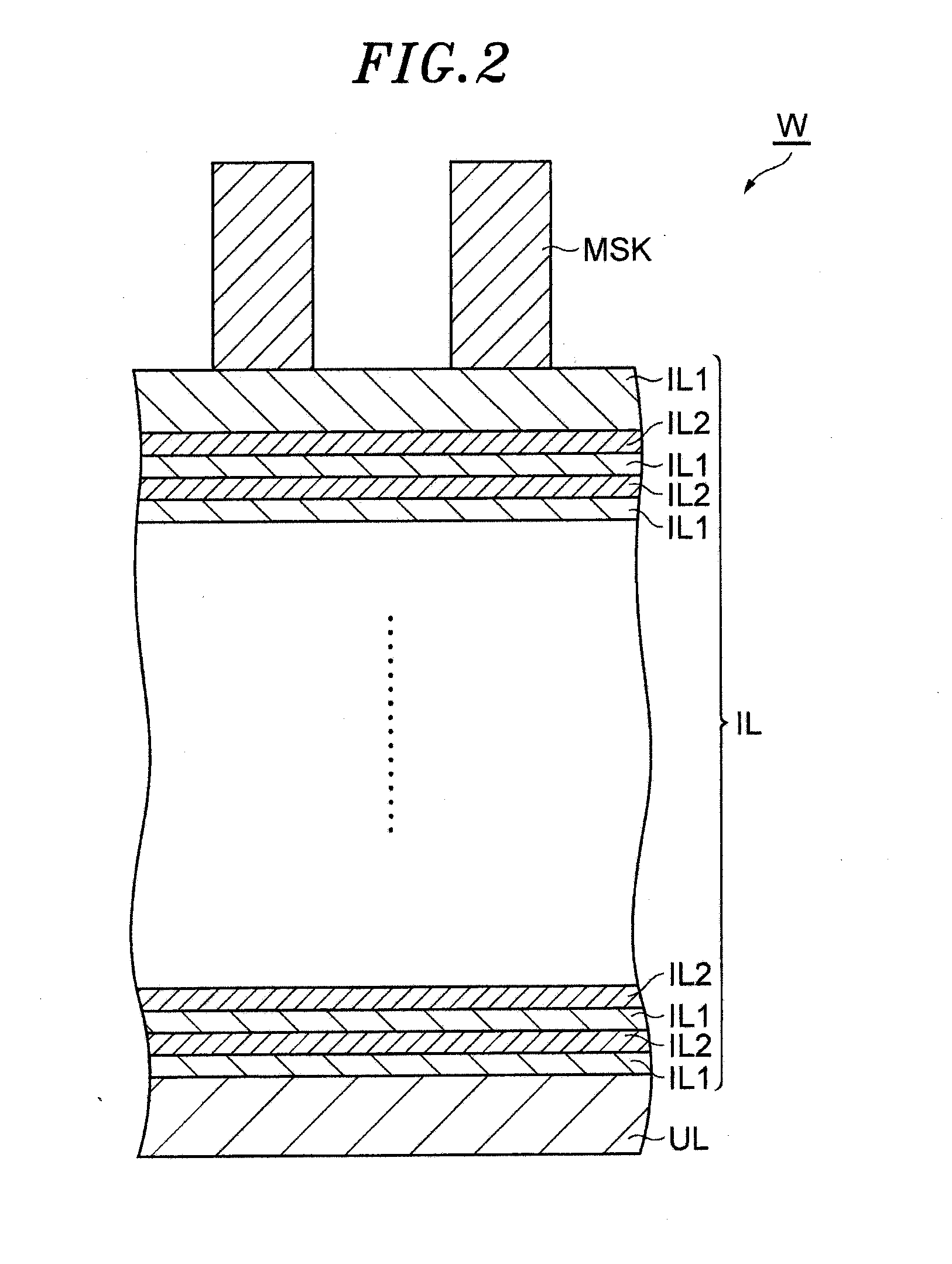
[0024]FIG. 2 shows an example of a wafer prepared in the step ST1. The wafer W shown in FIG. 2 includes a base layer UL, a multilayer film IL, and a mask MSK. The base layer UL may be a polycrystalline silicon layer formed on a substrate. The multilayer film IL is formed on the base layer UL. The multilayer fil...


PUM


Abstract

In a semiconductor device manufacturing method, a target object including a multilayer film and a mask formed on the multilayer film is prepared in a processing chamber of a plasma processing apparatus. The multilayer film is formed by alternately stacking a silicon oxide film and a silicon nitride film. The multilayer film is etched by supplying a processing gas containing hydrogen gas, hydrogen bromide gas, nitrogen trifluoride gas and at least one of hydrocarbon gas, fluorohydrocarbon gas and fluorocarbon gas into the processing chamber of the plasma processing apparatus and generating a plasma of the processing gas in the processing chamber.

Description

CROSS-REFERENCES TO RELATED APPLICATIONS[0001]The present invention claims priority of Japanese Patent Application Nos. 2013-159005 and 2014-020626 filed on Jul. 31, 2013 and Feb. 5, 2014, respectively, the entire contents of which are incorporated herein by reference.FIELD OF THE INVENTION[0002]An embodiment of the present invention relates to a semiconductor device manufacturing method.BACKGROUND OF THE INVENTION[0003]As an example of a semiconductor device, there is known a NAND-type flash memory device having a 3D structure. In the manufacture of the NAND-type flash memory device having a 3D structure, a multilayer film, which is formed by stacking two layers having different dielectric constant alternately, is etched to form a deep hole in the multilayer film. Such etching is disclosed in U.S. Patent Application Publication No. 2013 / 0059450.[0004]Specifically, referring to U.S. Patent Application publication No. 2013 / 0059450, the multilayer film is etched by exposing a target o...

Claims


Application Information

Patent Timeline
Patent Type & Authority Applications(United States)
IPC IPC(8): H01L21/311H01L21/033
CPCH01L21/31116H01L21/31144H01L21/0332H01J37/32091
Inventor OGAWA, KAZUTONARISHIGE, KAZUKISATO, TAKANORI
Owner TOKYO ELECTRON LTD
Why Eureka
Try Eureka