
Passive microwave device and method for producing the same

a microwave and passive technology, applied in the direction of resistor manufacturing, semiconductor devices, varistors, etc., can solve the problems of reducing the ability of the device to fully absorb rf energy and convert it into heat, increasing the physical size of the device, and reducing the usefulness of tuning networks over wide bandwidths

Inactive Publication Date: 2006-10-19
SMITHS INTERCONNECT MICROWAVE COMPONENTS
View PDF4 Cites 7 Cited by
  • Summary
  • Abstract
  • Description
  • Claims
  • Application Information

AI Technical Summary

Benefits of technology

[0006] Generally, the present invention provides an electrical circuit component, more specifically a passive RF/microwave device and a method for producing the same. In one embodiment, the present invention provides an electrical circuit component comprising: at least one patterned resistive area on a first surface of a diamond substrate, a first plurality of patterned conductive areas on the first surface of the diamond substrate, and a second plurality of patterned cond

Problems solved by technology

Even though BeO and AlN are used to dissipate large amounts of power due to their superior thermal properties, there are practical limitations as to how much power can be dissipated over any particular frequency range.
However, at high gigahertz frequencies, increasing the physical size of the device reduces its ability to fully absorb RF energy and convert it to heat.
However, tuning networks have limited usefulness over wide bandwidths.
Thus, there is no practical way of producing chip resistors, attenuators and terminations on conventional substrates such as alumina, BeO, and AlN that have both high power capability and wide bandwidth at high gigahertz frequencies.
Yet, as practical uses continue to be discovered for devices operating at high gigahertz frequencies, the general lack of passive devices having the necessary frequency and power handling capabilities required by these new and novel applications has become a real impediment to the widespread use of such new technology.

Method used


Image

  • Passive microwave device and method for producing the same
  • Passive microwave device and method for producing the same
  • Passive microwave device and method for producing the same

Examples


Embodiment Construction

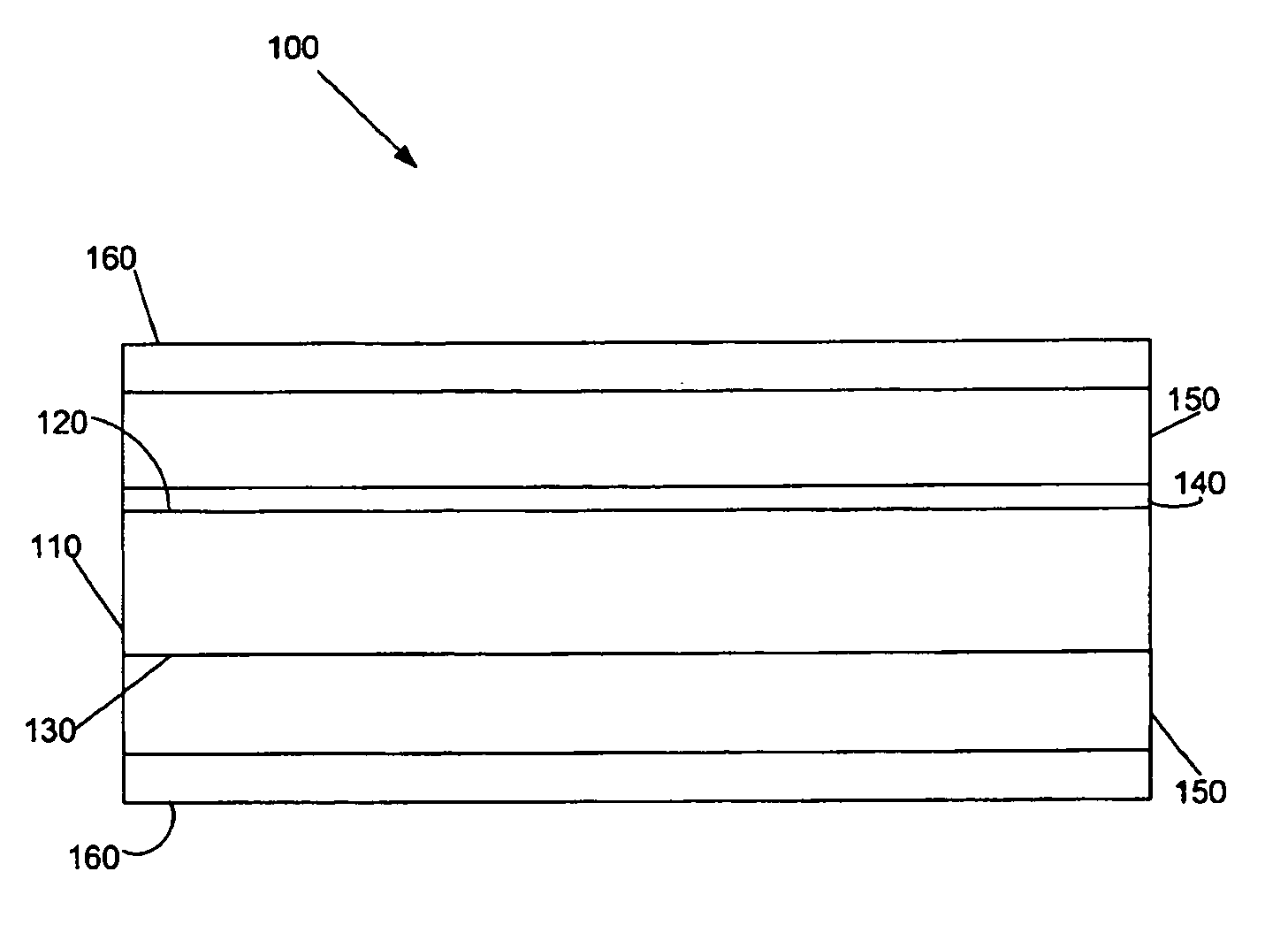
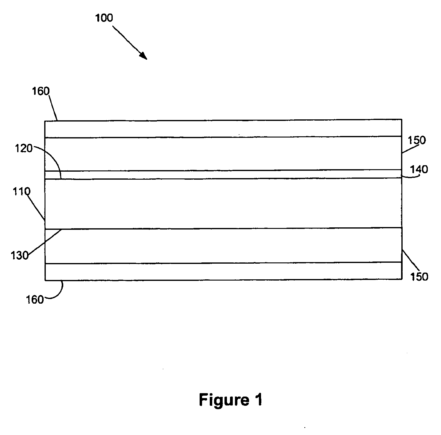
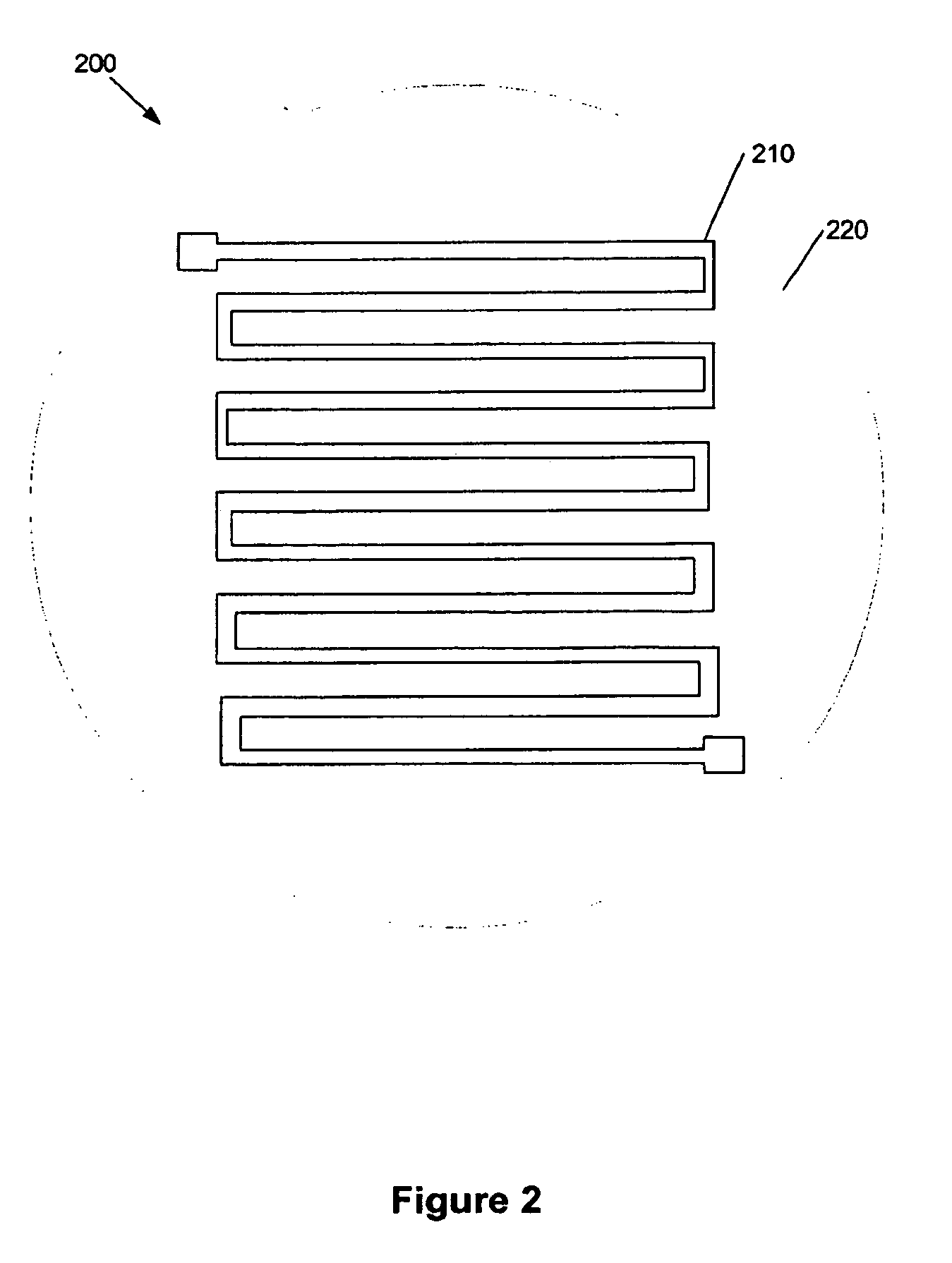
[0009] Generally, the present invention provides a passive microwave device and a method for producing the same. By way of example, the passive microwave device can be a resistor, termination, attenuator, power divider, coupler, temperature variable attenuator (TVA), or power sensing termination (PST). The device can handle microwave frequencies of about 1 to 100 GHz and the power requirements associated with the use of such microwave frequencies, such as 1 to 500 watts. Moreover, it can be embodied in a small and efficient package. The following text in connection with the figures describes various embodiments of the present invention. The following description, however, is not intended to limit the scope of the present invention. It should be appreciated where the same numbers are used in different figures, they refer to the same structure or element.

[0010]FIG. 1 is a side view of a coated passive device 100 formed in accordance with the invention. The coated passive device 100 c...


PUM


Abstract

The present invention provides an electrical circuit component, specifically a passive microwave device, and a method for producing the same. In one embodiment, the present invention provides an electrical circuit component, comprising: at least one patterned resistive area on a first surface of a diamond substrate, a first patterned conductive area on the first surface of the diamond substrate, and a second patterned conductive area on a second surface of the diamond substrate. The patterned resistive area may comprise a very thin film of tantalum nitride or a very thin film of tantalum nitride and a thin film of nichrome. The patterned conductive area may comprise a layer of titanium-tungsten, a layer of gold, and optionally a layer of nickel. Alternatively, the patterned conductive area may comprise a layer of chrome, a layer of copper, a layer of gold, and optionally a layer of nickel.

Description

FIELD OF THE INVENTION [0001] The invention relates to a passive RF / microwave device and a method for producing the same. BACKGROUND OF THE INVENTION [0002] The majority of passive microwave devices produced today are constructed with aluminum oxide (Al2O3), beryllium oxide (BeO), or aluminum nitride (AlN) substrates. These substrate materials have been chosen because of their particular mechanical, thermal, and / or electrical properties, as well as cost and environmental considerations. For example, the selection of alumina is due to its good mechanical strength and relatively low cost. BeO is used when superior thermal properties and low dielectric constants are needed. When high thermal conductivity is required without the environmental problems associated with BeO, AlN substrates are selected. [0003] Resistors, attenuators, and terminations are common applications of passive microwave devices. These types of devices are designed to convert excess RF energy into heat. Generally, t...

Claims


Application Information

Patent Timeline
IPC IPC(8): H01L29/00
CPCH01C7/1013H01L27/016H01C17/075
Inventor BLACKA, ROBERT J.PERSCHNICK, GENE A.WRIGHT, ROBERT
Owner SMITHS INTERCONNECT MICROWAVE COMPONENTS
Learn More