Multilevel semiconductor module and method for fabricating the same

a semiconductor module and multi-level technology, applied in the direction of semiconductor devices, semiconductor/solid-state device details, electrical apparatus, etc., can solve the problems of partial failure of packaging, semiconductor module warp, and occurrence of entire semiconductor module warp suppression, and achieve cost reduction of electronic equipment, high reliability, and effect of suppressing the effect of entire semiconductor module warp

Inactive Publication Date: 2006-10-19
PANASONIC CORP
View PDF11 Cites 122 Cited by
  • Summary
  • Abstract
  • Description
  • Claims
  • Application Information

AI Technical Summary

Benefits of technology

[0007] In recent years, techniques for reducing the thickness of semiconductor chips by polishing and techniques for mounting the thin semiconductor chips on boards with high yields have been developed, so that the number of levels of such stacked semiconductor chips has been further increasing. In addition, in a semiconductor memory, for example, as the memory capacity increases, the chip area increases. If a module is formed by stacking large semiconductor chips in multiple levels, the problem of a warp of the module arises. As the thickness of a printed board decreases, the degree of warp of the module increases. Accordingly, to stack printed boards on which semiconductor chips are mounted and interlayer members in multiple levels, it is important to suppress the occurrence of a warp.
[0010] To solve the foregoing problems, the methods described above only provide structures in which boards on which semiconductor chips of the same shape are respectively mounted and include processes for forming the structures. However, no measures are taken to suppress a warp of a semiconductor module formed by stacking the boards and to enhance moisture resistance reliability of the semiconductor module.
[0013] In the multilevel semiconductor module of the present invention, the resin board at the bottom is thicker than the other resin boards, thereby suppressing occurrence of a warp of the entire multilevel semiconductor module. In addition, the exposed part of the semiconductor chip is covered with the adhesive member or a resin material having a low softening point and a low stiffness, so that water, moisture and corrosive gas, for example, causing corrosion of a wire material used for the semiconductor chips and the resin boards are blocked, thereby preventing occurrence of failures due to disconnection of wires.
[0014] A portion of the adhesive member located above the opening preferably has a thickness larger than the other portion. Then, the semiconductor chip is more securely covered and the number of components is reduced. The multilevel semiconductor module of this embodiment can be modified in various manners. For example, the diameter of some of the first and second buried members may be increased or a rigid plate may be attached to the module. In a structure in which the semiconductor chip is mounted with the back surface thereof facing the resin board, the semiconductor chip may be encapsulated with a resin.
[0018] With this method, the upper and side faces of the semiconductor chip are covered at the step (c) before the step (d) at which the components are united, thus ensuring covering of the semiconductor chip.
[0019] In the multilevel semiconductor module of the present invention, the resin board located at the bottom and connected to the external boards out of the stacked resin boards is thicker than the other boards, so that occurrence of a warp of the entire semiconductor module is suppressed. Accordingly, even if the number of terminals is increased, the module is coupled to a mother board with high reliability and functional enhancement and cost reduction of electronic equipment are effectively achieved. In addition, since the exposed parts of the semiconductor chips are covered with, for example, the adhesive members, moisture and corrosive gas, for example, are prevented from entering. Accordingly, failures are less likely to occur as compared to a conventional semiconductor module.

Problems solved by technology

If a module is formed by stacking large semiconductor chips in multiple levels, the problem of a warp of the module arises.
Accordingly, if a warp occurs at room temperature or is caused by heating during bonding, a semiconductor module cannot be mounted on the mother board or the warp causes a partial failure in packaging.
That is, a semiconductor module can be defective in packaging though it is non-defective in its electric characteristics.
However, considering the structure formed by stacking circuit boards on which semiconductor chips are mounted, it is difficult to obtain high moisture resistance reliability enough to stand rigorous conditions, as compared to general semiconductor devices.
However, no measures are taken to suppress a warp of a semiconductor module formed by stacking the boards and to enhance moisture resistance reliability of the semiconductor module.

Method used


Image

  • Multilevel semiconductor module and method for fabricating the same
  • Multilevel semiconductor module and method for fabricating the same
  • Multilevel semiconductor module and method for fabricating the same

Examples


embodiment 1

—Configuration of Semiconductor Module—

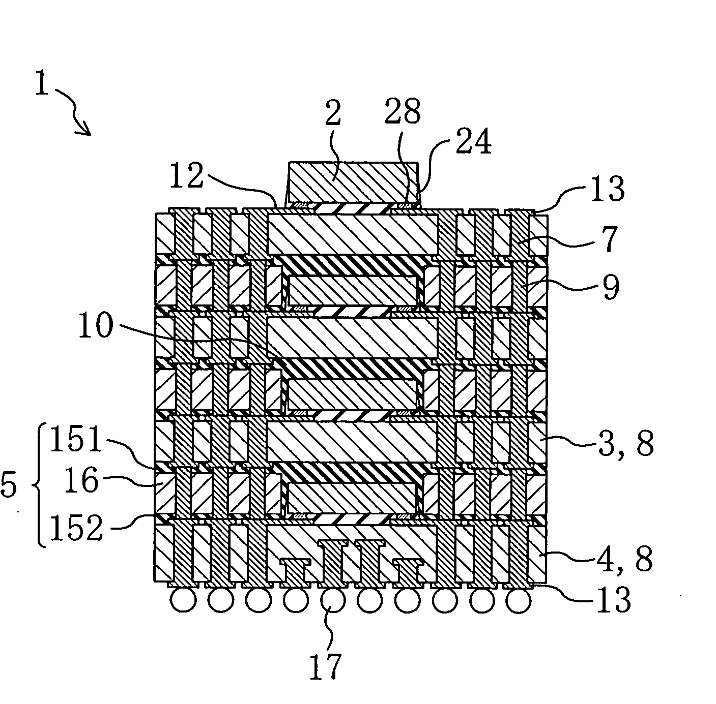
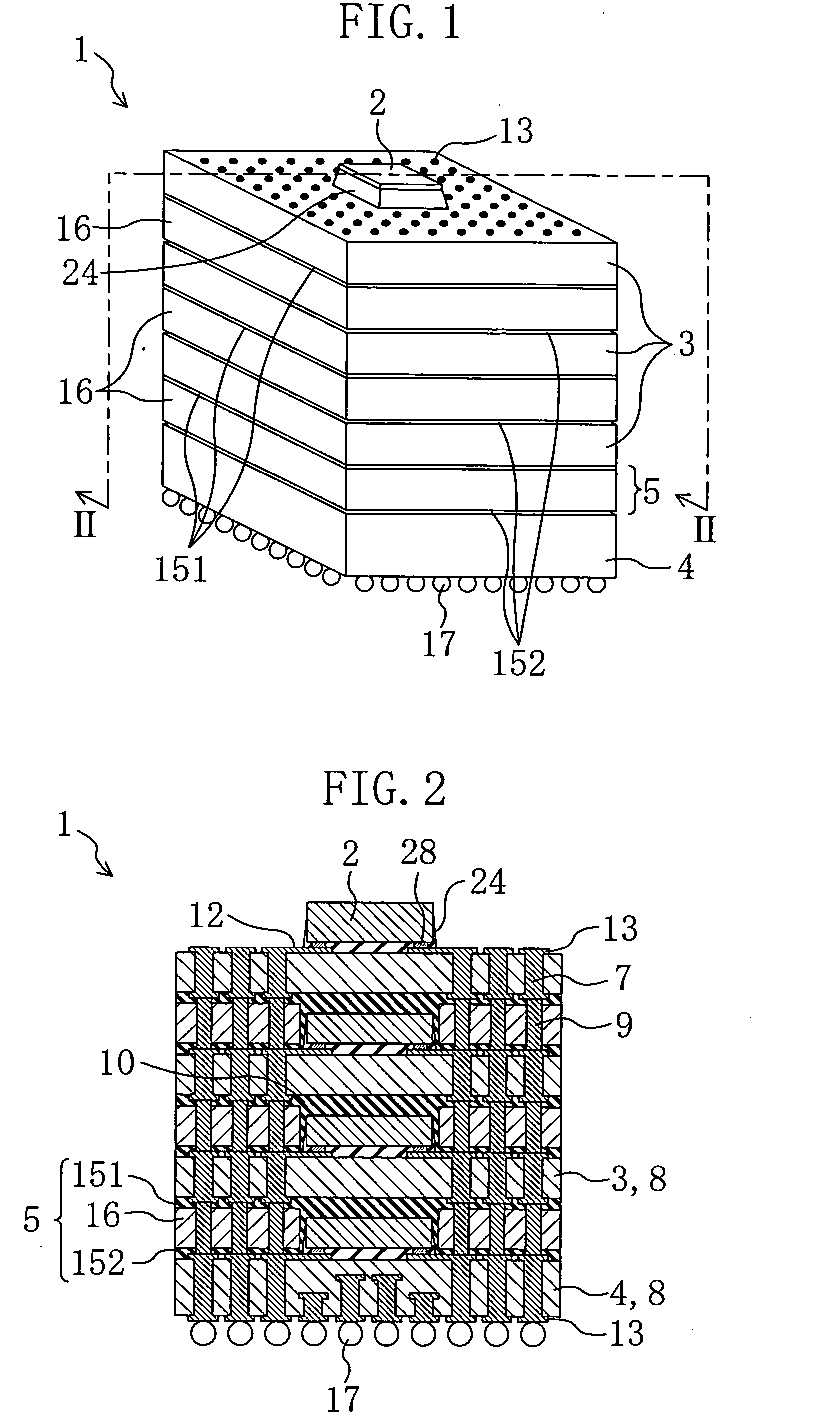
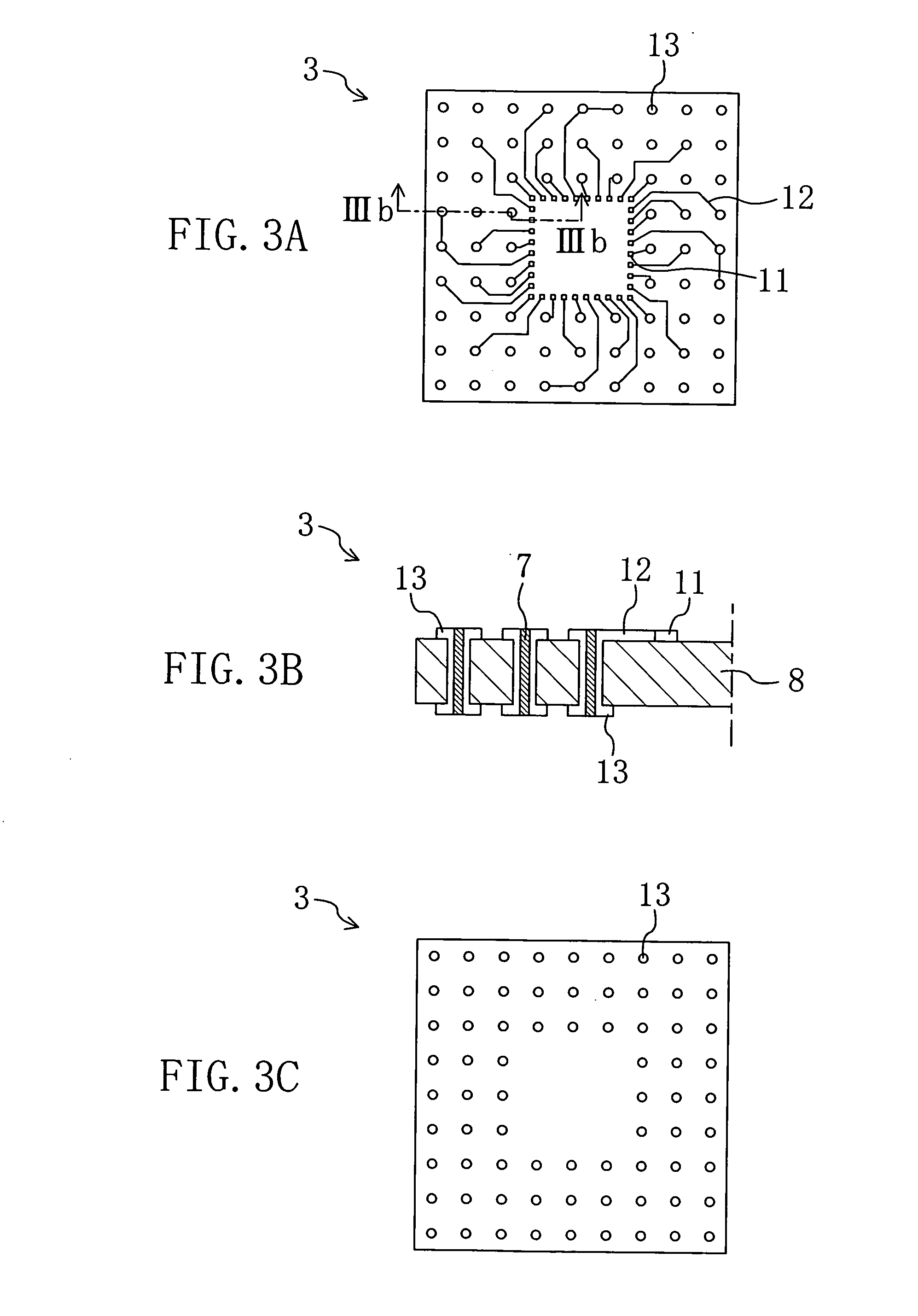
[0049]FIG. 1 is a perspective view schematically illustrating an overall configuration of a multilevel semiconductor module according to a first embodiment of the present invention. FIG. 2 is a cross-sectional view of the multilevel semiconductor module of this embodiment taken along the line II-II in FIG. 1. FIG. 3A is a plan view schematically illustrating the upper face of a resin board used in the multilevel semiconductor module of this embodiment. FIG. 3B is a cross-sectional view of the resin board of this embodiment taken along the line IIIb-IIIb in FIG. 3A. FIG. 3C is a plan view schematically illustrating the lower face of the resin board of this embodiment. FIGS. 4A and 4B are a plan view illustrating an example of an adhesive member included in a sheet member used in the multilevel semiconductor module of this embodiment and a cross-sectional view illustrating an adhesive member taken along the line IVb-IVb, respectively. FIGS. 4C an...

embodiment 2

[0116] Hereinafter, a multilevel semiconductor module 100 according to a second embodiment of the present invention will be described with reference to FIG. 11 through FIG. 14.

—Configuration of Semiconductor Module—

[0117]FIG. 11 is a perspective view schematically illustrating an overall configuration of a multilevel semiconductor module 100 according to this embodiment. FIG. 12 is a cross-sectional view of the multilevel semiconductor module of this embodiment taken along the line XII-XII in FIG. 11. In these drawings, the thicknesses and lengths, for example, of components of the semiconductor module are selected so as to be easily shown, and therefore are different from those of actual components. The numbers and shapes of buried conductors and external connection terminals for external connection are different from those of actual conductors and terminals and are selected to be easily shown in the drawings. This is also applied to the other drawings. In FIGS. 11 and 12, compone...

embodiment 3

[0148] Hereinafter, a multilevel semiconductor module 110 according to a third embodiment of the present invention will be described with reference to FIGS. 15 through 18.

[0149]FIG. 15 is a perspective view schematically illustrating an overall configuration of a multilevel semiconductor module according to the third embodiment. FIG. 16 is a cross-sectional view of the semiconductor module of this embodiment taken along the line XVI-XVI in FIG. 15. In FIGS. 15 and 16, components already described in the first and second embodiments are denoted by the same reference numerals in FIGS. 1 and 2 and FIGS. 11 and 12.

—Configuration of Semiconductor Module—

[0150] As illustrated in FIGS. 15 and 16, the semiconductor module 110 of this embodiment includes a second resin board 4 on which a semiconductor chip 2 is mounted and a stacked structure provided on the second resin board 4. The stacked structure is formed by alternately stacking sheet members 5 provided with openings 10 for housing s...


PUM


Abstract

A semiconductor module is formed by alternately stacking resin boards and sheet members. Each of the resin boards includes first buried conductors. A semiconductor chip is mounted on the upper face of each of the resin boards. Each of the sheet members having an opening for accommodating the semiconductor chip and including second buried conductors electrically connected to the first buried conductors. A first resin board located at the bottom is thicker than second resin boards. Each of the sheet members includes an adhesive member covering the upper and side faces of the semiconductor chip.

Description

FIELD OF THE INVENTION [0001] The present invention relates to three-dimensional multilevel semiconductor modules formed by alternately stacking sheet members and resin boards on which semiconductor chips are mounted and also relates to methods for fabricating the modules. DESCRIPTION OF THE RELATED ART [0002] With demands for size reduction and performance improvement of various electronic devices such as cellular phones and digital cameras, multilevel semiconductor modules formed by stacking and uniting a plurality of electronic components, especially semiconductor chips, have been proposed. [0003] Methods for easily manufacturing such multilevel semiconductor modules at low cost have been proposed to date. [0004] A conventional semiconductor module is formed by stacking, as one unit, a printed board on which a given circuit is formed, a semiconductor chip mounted on the printed board, and an interlayer member that has an opening capable of accommodating the semiconductor chip and...

Claims


Application Information

Patent Timeline
Patent Type & Authority Applications(United States)
IPC IPC(8): H01L23/02
CPCH01L23/5385H01L2225/1023H01L25/0657H01L25/105H01L2224/16H01L2224/48091H01L2224/48227H01L2225/0651H01L2225/0652H01L2225/06541H01L2225/06555H01L2225/06572H01L2924/01078H01L2924/01079H01L2924/15311H01L2924/30107H01L2924/3011H01L23/5389H01L2225/107H01L24/48H01L2224/73265H01L2924/3511H01L2224/73204H01L2224/32225H01L2224/16225H01L2924/00014H01L2924/00012H01L2924/00H01L2224/451H01L2224/45124H01L2224/45144H01L2224/45147H01L24/45H01L24/73H01L2924/1627H01L2924/181H01L2224/05599H01L23/12H01L25/03
Inventor KAWABATA, TAKESHISATOU, MOTOAKIFUKUDA, TOSHIYUKITSUDA, TOSHIONOBORI, KAZUHIRONAKATANI, SEIICHI
Owner PANASONIC CORP
Why Eureka
Try Eureka