Method for monitoring a reticle

a technology of reticles and reticles, applied in the direction of photomechanical equipment, instruments, originals for photomechanical treatment, etc., can solve the problems that the defect formed on the wafer during lithography may be particularly problematic for the integrated circuit manufacturing process

Inactive Publication Date: 2006-10-19
KLA TENCOR TECH CORP
View PDF7 Cites 19 Cited by
  • Summary
  • Abstract
  • Description
  • Claims
  • Application Information

AI Technical Summary

Benefits of technology

[0011] In another implementation, performing the inspection indicates whether the reticle has been adversely affected by repeated exposure to radiation. In a f...

Problems solved by technology

Consequently, defects that are formed on the wafer during lithography ma...

Method used


Image

  • Method for monitoring a reticle
  • Method for monitoring a reticle
  • Method for monitoring a reticle

Examples


Embodiment Construction

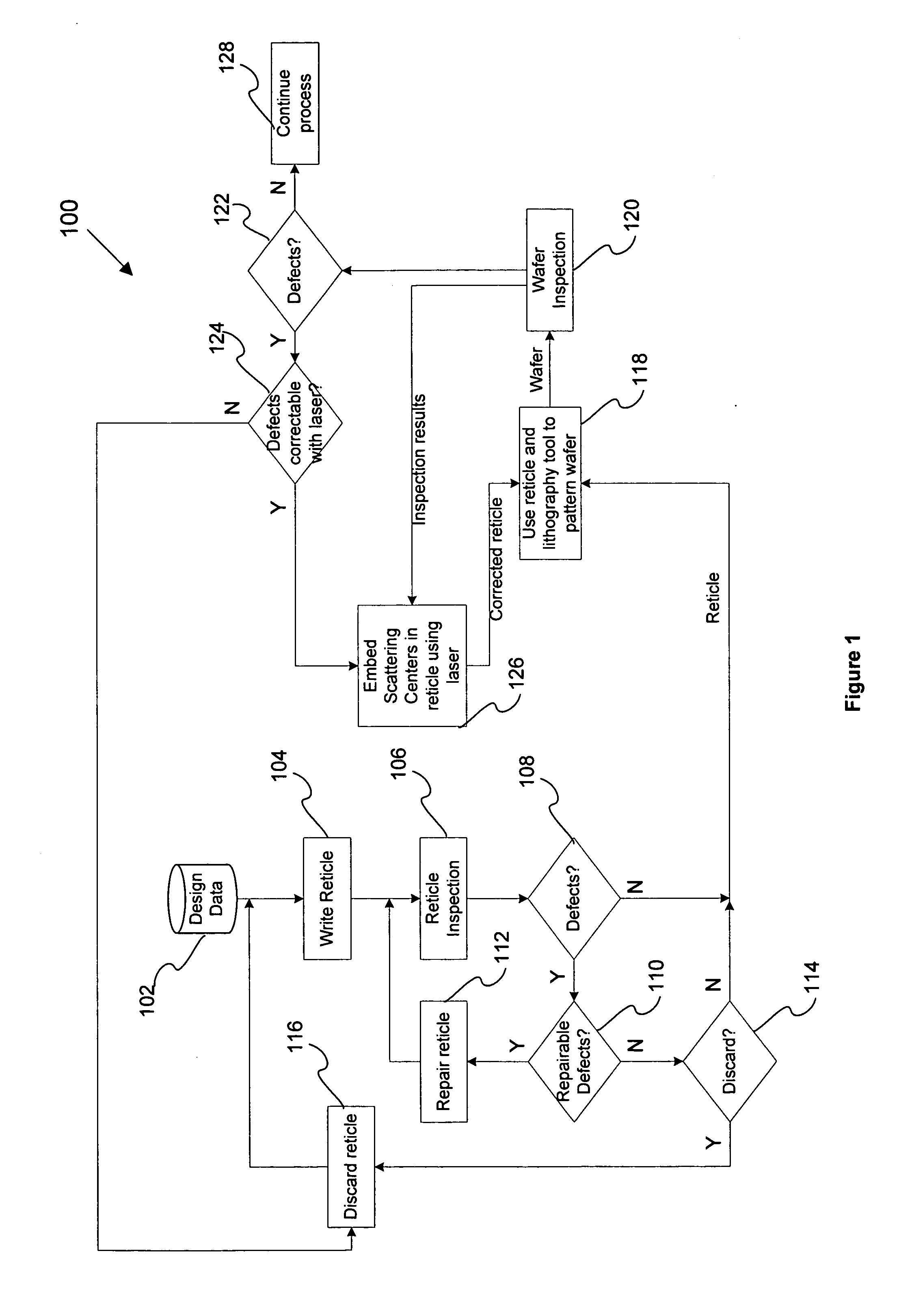
[0021] Reference will now be made in detail to a particular embodiment of the invention, examples of which are illustrated in the accompanying drawings. While the invention will be described in conjunction with the particular embodiments, it will be understood that it is not intended to limit the invention to the described embodiments. To the contrary, it is intended to cover alternatives, modifications, and equivalents as may be included within the spirit and scope of the invention as defined by the appended claims.

[0022] The terms “reticle” and “mask” are used interchangeably herein. A reticle generally includes a transparent substrate such as glass, borosilicate glass, and fused silica having a layer of opaque material formed thereon. A reticle may include additional materials formed under the opaque material such as an adhesion layer. In addition, a reticle may include additional materials formed on top of the opaque material such as a bottom anti-reflective coating, a resist (...


PUM


Abstract

Reticles may comprise shading elements (SEs) for locally altering the reticle optical properties. However, such reticles may degrade over time as a result of repeated exposure to radiation in a lithography process, as the radiation may “heal” the SEs. Disclosed are techniques for monitoring a reticle in order to maintain confidence about the reticle's optical properties and the uniformity of patterns on wafers that are to be printed using the reticle. Reticles undergo periodic inspection comprising reticle transmission measurement and/or aerial imaging of the reticle. When such inspection indicates sufficient reticle degradation, the reticle is tagged for correction prior to its subsequent use in a lithography process.

Description

CROSS REFERENCE TO RELATED PATENT APPLICATION [0001] This application claims priority of U.S. Provisional Patent Application Nos. U.S. Provisional Application No. 60 / 671,150 (Attorney Docket No. KLA1P151P), entitled “METHOD FOR MONITORING A RETICLE”, filed 13 Apr. 2005 by Sterling G. Watson et al., which application is incorporated herein by reference in its entirety for all purposes.FIELD OF INVENTION [0002] The invention pertains in general to integrated circuit design and fabrication, and in particular to monitoring reticles. BACKGROUND [0003] Fabricating semiconductor devices such as logic and memory devices typically includes processing a substrate such as a semiconductor wafer using a number of semiconductor fabrication processes to form various features and multiple levels of the semiconductor devices. For example lithography is a semiconductor fabrication process that involves transferring a pattern from a reticle to a resist arranged on a semiconductor wafer. Additional exa...

Claims


Application Information

Patent Timeline
IPC IPC(8): G03F1/00G03C5/00G06K9/00
CPCG03F1/14G03F1/144G03F1/38Y10S430/146G03F1/84G03F7/70433G03F7/70625G03F1/50
Inventor WATSON, STERLING G.LEVY, ADYMACK, CHRIS A.STOKOWSKI, STANLEY E.SAIDIN, ZAIN K.
Owner KLA TENCOR TECH CORP
Why Eureka
Try Eureka