Field-effect transistor

a field-effect transistor and transistor technology, applied in the direction of transistors, electrical devices, semiconductor devices, etc., can solve the problems of difficult to form a high-quality p-type layer, the transistor itself breaks down, and the difficulty of forming an n-type region within a p-type layer

Inactive Publication Date: 2006-10-26
SHARP KK
View PDF3 Cites 24 Cited by
  • Summary
  • Abstract
  • Description
  • Claims
  • Application Information

AI Technical Summary

Problems solved by technology

If the gate voltage Vg is reduced to zero for some cause in a normally-on FET, on the other hand, overcurrent can flow between the source and drain, and there is a possibility that the transistor itself breaks down.
In the case of GaN, however, it is not easy to form a high-quality p-type layer and it is very difficult to form an n-type region within a p-type layer by ion implantation or diffusion, dissimilarly to the case of Si.
Therefore, a MOSFET including no hetero-structure (e.g., GaN-MOSFET) has not yet been put into practice.
As described before, however, it is difficult to prepare a normally-off field-effect transistor including a hetero-structure.

Method used


Image

  • Field-effect transistor
  • Field-effect transistor
  • Field-effect transistor

Examples


embodiment 1

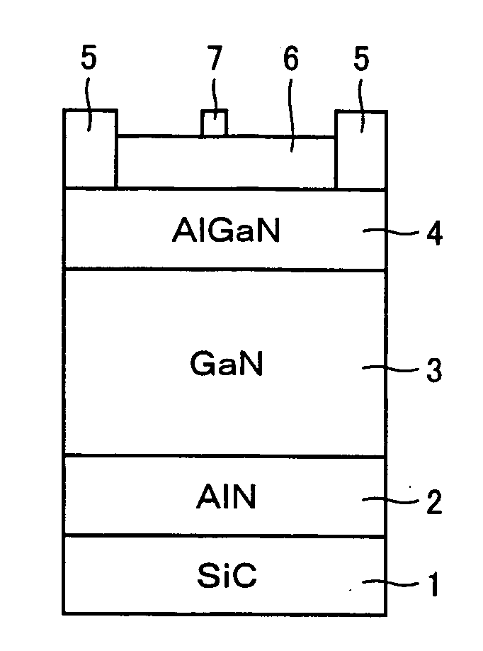
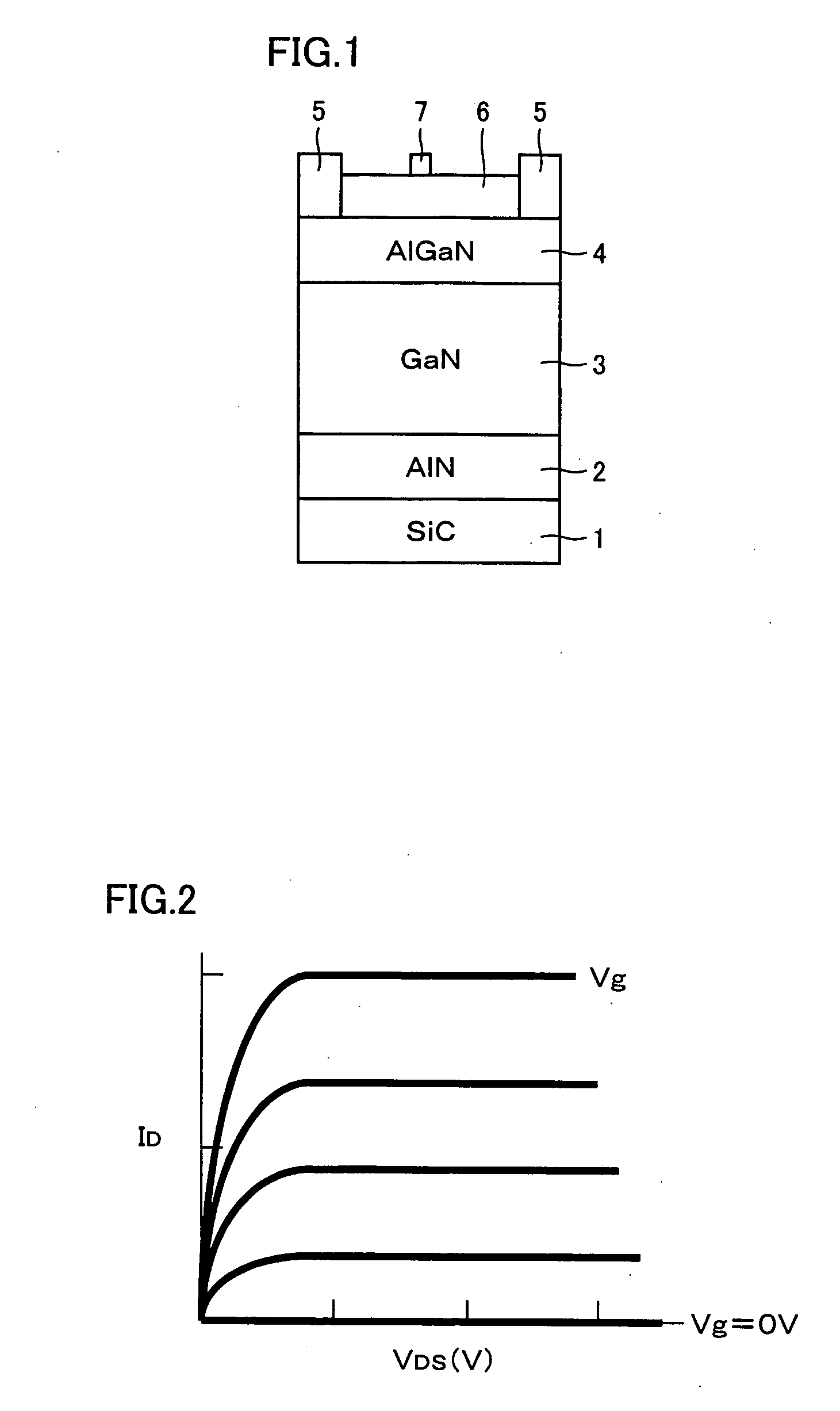
[0037]FIG. 1 is a schematic sectional view showing a hetero-junction FET according to Embodiment 1 of the present invention. In order to prepare this FET, an AlN buffer layer 2 having a thickness of 20 nm is grown on an Si atomic plane of an SiC substrate 1 by MOCVD (metal organic chemical vapor deposition) at a substrate temperature of 1200° C. Then, a GaN channel layer 3 having a lattice constant a=3.189 Å and a band gap Eg=3.42 eV is grown to a thickness of 3 μm on AlN buffer layer 2 at a substrate temperature of 1100° C. Then, an Al0.3Ga0.7N barrier layer 4 having a lattice constant a=3.166 Å and a band gap Eg=4.02 eV is grown to a thickness of 20 nm on GaN channel layer 3 at a substrate temperature of 1100° C.

[0038] Thereafter, in order to form source and drain electrodes 5a, a resist film is patterned by photolithography; a multilayer metal film is deposited including Hf (10 nm thickness) / Al(100 nm thickness) / Hf(40 nm thickness) / Au(240 nm thickness) layers stacked in this ord...

embodiment 2

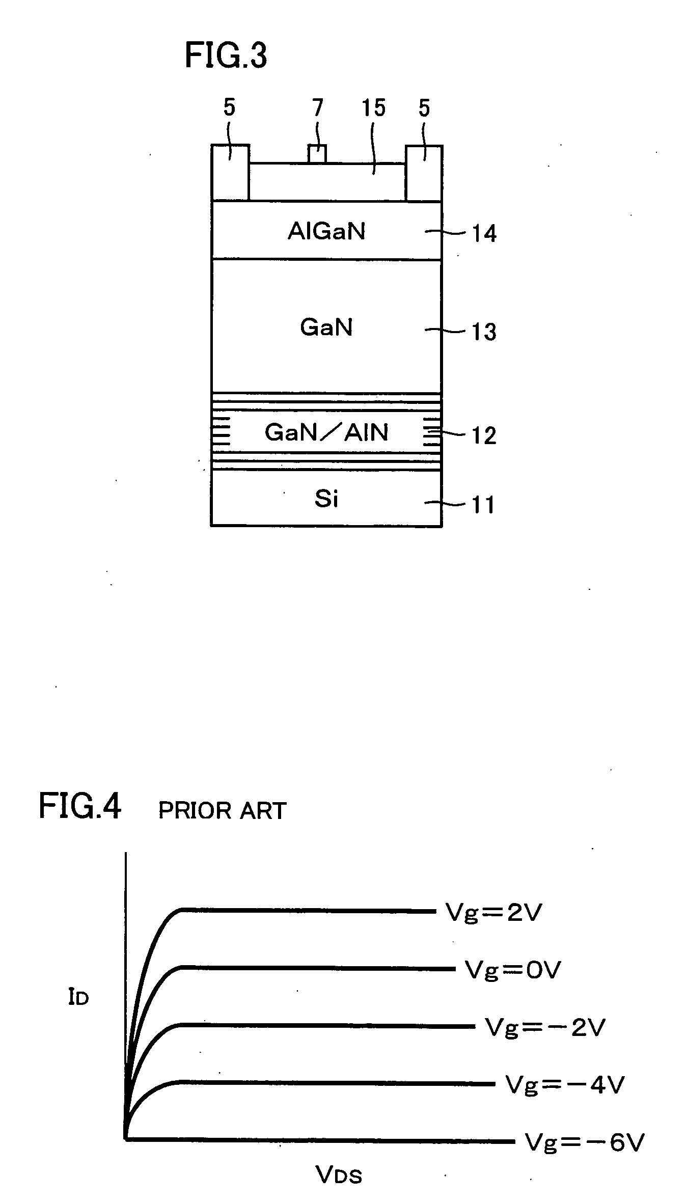
[0040]FIG. 3 is a schematic sectional view showing a structure of an FET including a hetero-structure according to Embodiment 2 of the present invention. In this FET, an Si substrate 11 is used for depositing an AlN / GaN multilayer film as a buffer layer 12, growing a GaN layer of 1 μm thickness having a lattice constant a=3.189 Å and a band gap Eg=3.42 eV as a channel layer 13 at a substrate temperature of 1000° C., and growing an Al0.2Ga0.8N layer of 30 nm thickness having a lattice constant a=3.174 Å and a band gap Eg=3.80 eV as a barrier layer 14 at a substrate temperature of 1100° C. When an AlN layer or a GaN layer is grown on Si substrate 11, an Al atomic plane or a Ga atomic plane appears on its upper surface (the side on which electrodes are to be formed).

[0041] An oxide film or a fluoride film serving as a piezoelectric effect film 15 can be deposited by sputtering also in Embodiment 2, similarly as in the case of Example 1. The sputtering can be carried out by using Ar an...

embodiment 3

[0043]FIG. 7 is a schematic sectional view showing a structure of an FET including a hetero-structure according to Embodiment 3 of the present invention. While the GaN layer and the AlGaN barrier layer are so stacked that a Ga atomic plane of each of the layers appears on the upper surface (the side on which electrodes are to be formed) in each of the aforementioned Embodiments 1 and 2, a GaN layer 13 and an AlGaN layer 14 can alternatively be so stacked that an N atomic plane of each of the layers appears on the upper surfaces (the side on which electrodes are to be formed) as in this Embodiment 3.

[0044] In this case, a buffer layer 12 of AlN, a first semiconductor layer 14 of AlGaN and a second semiconductor layer 13 of GaN are stacked in this order on a C atomic plane of an SiC substrate 11, as shown in FIG. 7. At this time, AlGaN layer 14 and GaN layer 13 have their respective lattice constants a1 and a2 in the relation a12 (i.e., the lattice constant a1 of AlGaN is reduced bel...


PUM


Abstract

A nitride-based group III-V compound semiconductor device includes a buffer layer, a first nitride semiconductor layer and a second nitride semiconductor layer successively stacked on a substrate, the first and the second nitride layers having their respective lattice constants a1 and a2 in the relation a1>a2, an ohmic source electrode and an ohmic drain electrode formed on the second nitride layer, and a piezoelectric effect film formed on at least a partial region between the electrodes, wherein the piezoelectric film exerts compressive stress of an absolute magnitude at least equivalent to that of tensile stress applied to the second nitride layer due to the difference (a1−a2) between the lattice constants of the first and second nitride layers.

Description

[0001] This nonprovisional application is based on Japanese Patent Applications Nos. 2005-128241 and 2006-041138 filed with the Japan Patent Office on Apr. 26, 2005 and Feb. 17, 2006, respectively, the entire contents of which are hereby incorporated by reference. BACKGROUND OF THE INVENTION [0002] 1. Field of the Invention [0003] The present invention relates to a field-effect transistor (FET) composed of nitride-based group III-V compound semiconductors, and more particularly relates to a normally-off field-effect transistor. [0004] 2. Description of the Background Art [0005] A conventional field-effect transistor employing nitride-based group III-V compound semiconductors includes a GaN layer and an AlGaN layer stacked with each other on a substrate (refer to U.S. Pat. No. 5,192,987). The AlGaN layer has a smaller lattice constant as compared with the GaN layer. [0006] A field-effect transistor employing nitride-based group III-V semiconductors includes a hetero-structure of AlGa...

Claims


Application Information

Patent Timeline
Patent Type & Authority Applications(United States)
IPC IPC(8): H01L31/00
CPCH01L21/02378H01L21/02381H01L21/02458H01L21/02502H01L21/02507H01L29/7787H01L29/1029H01L29/2003H01L29/42316H01L29/7781H01L21/0254H01L21/18H01L29/768H01L29/772
Inventor TERAGUCHI, NOBUAKI
Owner SHARP KK
Why Eureka
Try Eureka