Semiconductor memory device and electronic equipment

a memory device and semiconductor technology, applied in static storage, digital storage, instruments, etc., can solve the problems of increasing the chip area on the contrary, affecting the operation of the memory device, so as to achieve the effect of simple configuration, high accuracy, and reliable electronic equipmen

Inactive Publication Date: 2006-10-26
SHARP KK
View PDF2 Cites 22 Cited by
  • Summary
  • Abstract
  • Description
  • Claims
  • Application Information

AI Technical Summary

Benefits of technology

[0079] Due to the provision of the semiconductor memory device which has a relatively simple configuration ...

Problems solved by technology

Because of this, there is a problem that for example at writing to one of adjacent memory cells, drain disturbance occurs in the other memory cell.
Because of this, there is a problem that the write time becomes extremely long.
In addition, the above semiconductor memory device in which the memory cell array is divided using transistors has a problem that it needs an area to form the transistors, thereby increasing the chip area on the contrary.
By the way, the information stored in a nonvolatile memory cell is determined with the help of variation in the cell currents responsive to the storage condition, it is difficult from a structure viewpoint to get perfect agreement of cell current between a plurality of memory cells in which the same information is stored.
However, if the distribution of cell current values of memory cells in which certain information is stored overlaps with the...

Method used


Image

  • Semiconductor memory device and electronic equipment
  • Semiconductor memory device and electronic equipment
  • Semiconductor memory device and electronic equipment

Examples


first embodiment

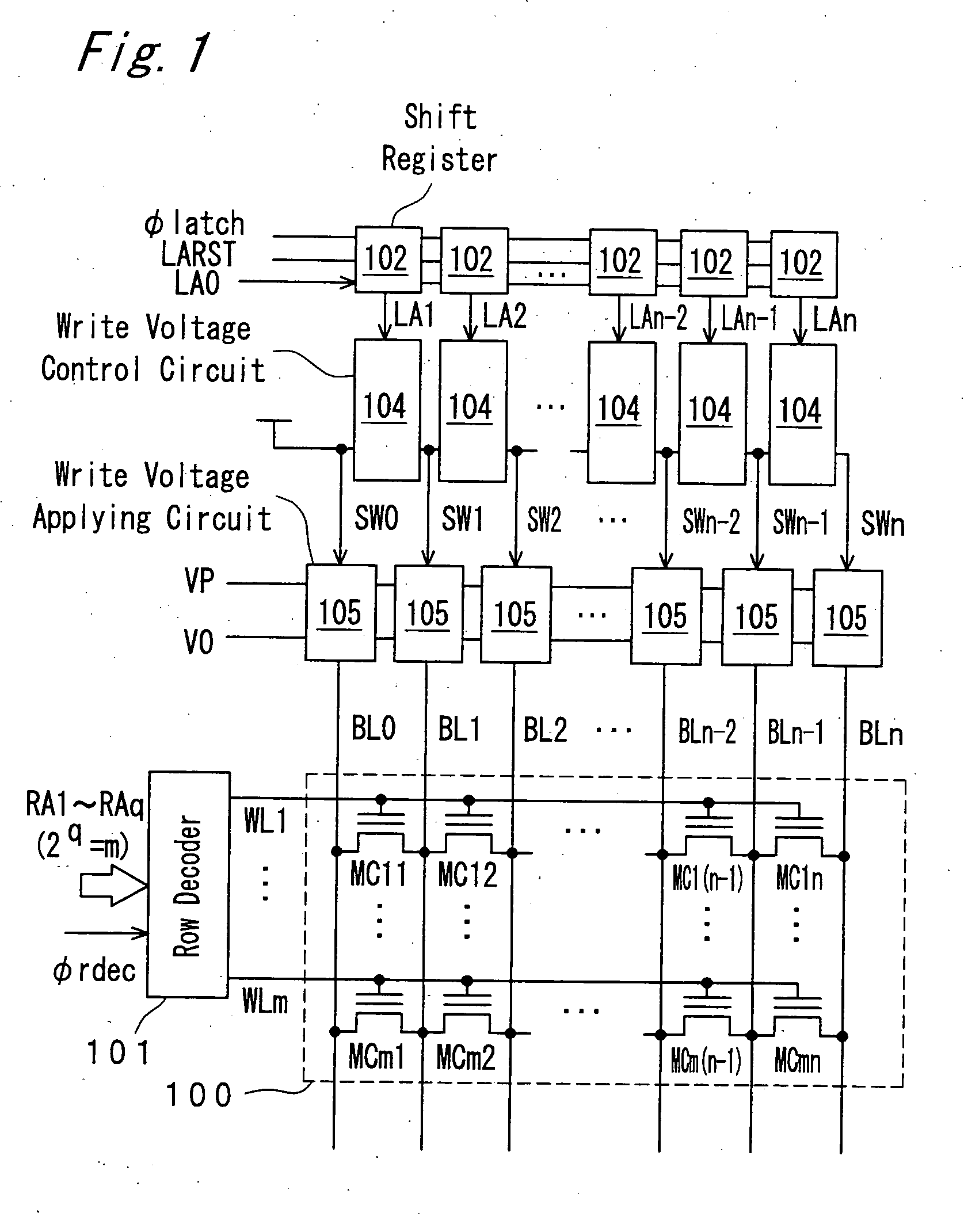
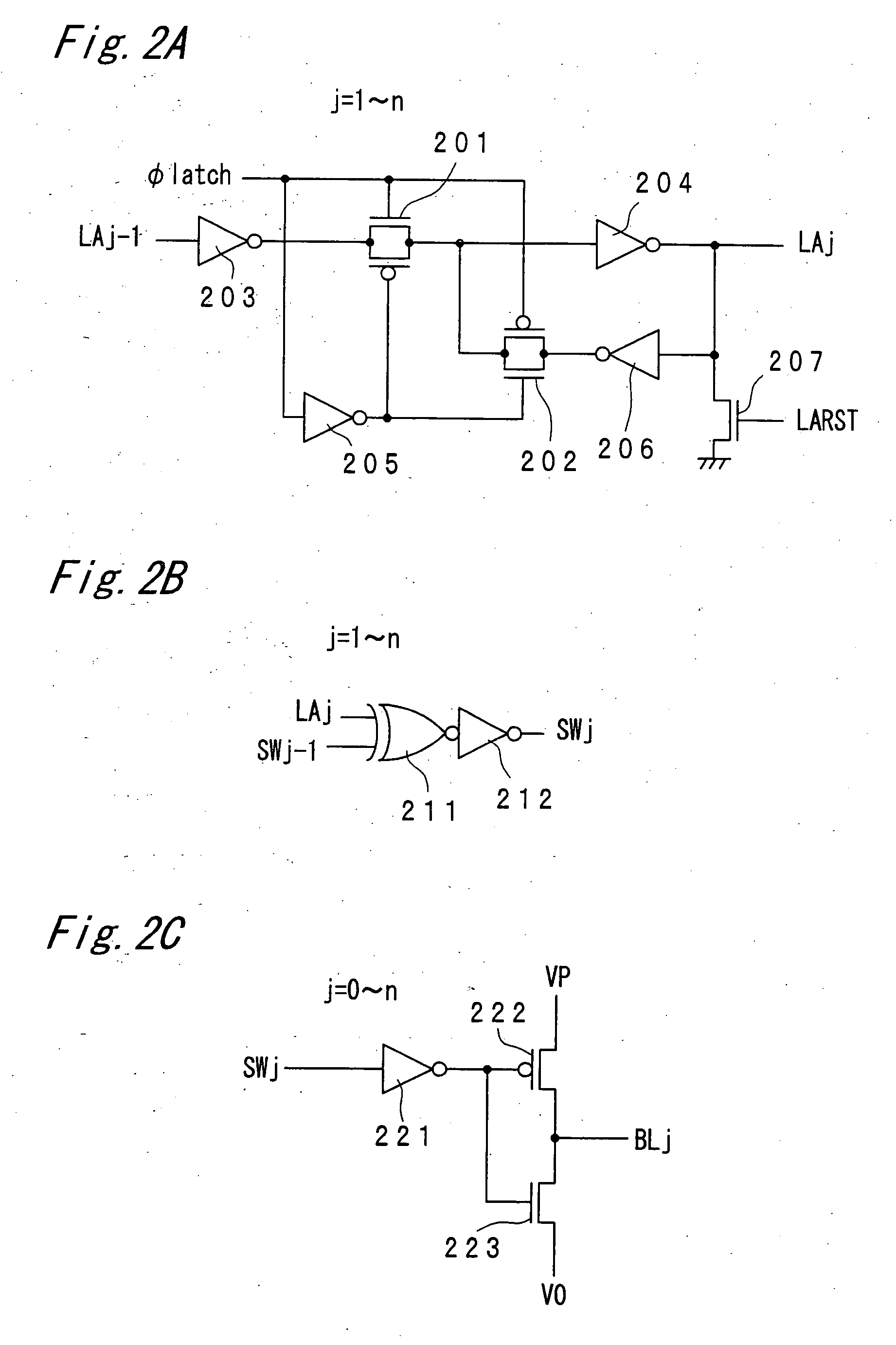
[0139]FIG. 1 is a block diagram showing a semiconductor memory device of the first embodiment of the present invention. FIGS. 2A and 2C are circuit diagrams showing an example of the peripheral circuits of the semiconductor memory device.

[0140] As shown in FIG. 1, this semiconductor memory device has a memory cell array 100 in which a plurality of nonvolatile memory cells MC11, MC12, - - - , MC1(n−1), MC1n, - - - , MCm(n−1), and MCmn are arranged in the form of a matrix. In this memory cell array 100, a plurality of word lines WL1 to WLm align in the column direction, and each of the word lines extends in the row direction and is connected with the control gates of the memory cells of a corresponding row. Furthermore, in the memory cell array 100, a plurality of bit lines BL0 to BLn align in the row direction, and each of the bit lines extends in the column direction and is connected with the input and output terminals, i.e., sources and drains of the memory cells of a correspondin...

second embodiment

[0152]FIG. 4 is a block diagram showing a semiconductor memory device of a second embodiment of the present invention, and FIGS. 5 and 6 are circuit diagrams showing an example of the peripheral circuits of the semiconductor memory device.

[0153] As shown in FIG. 4, this semiconductor memory device has a memory cell array 400 in which a plurality of nonvolatile memory cells MC111, MC112, - - - , MC11(n−1), MC11n, MC121, - - - , MCm11, - - - , MCm2n, - - - , and MCmrn are arranged in the form of a matrix. This memory cell array 400 has r areas each including n memory cells in the row direction. In this memory cell array 400, a plurality of word lines WL1 to WLm are arranged in the column direction, and each of the word lines extends in the row direction and is connected with the control gates of the memory cells aligning in the same row. Furthermore, in the memory cell array 400, a plurality of bit lines BL10 to BLrn are arranged in the row direction. Each of bit lines extends in the...

third embodiment

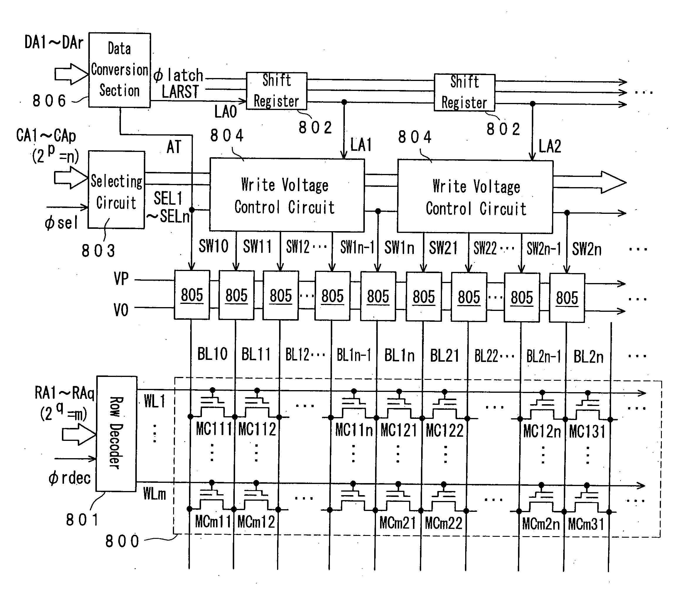
[0166]FIG. 8 is a block diagram showing a semiconductor memory device of a third embodiment of the present invention.

[0167] The semiconductor memory device of this embodiment has a memory cell array 800 in which a plurality of nonvolatile memory cells MC111, MC112, - - - , MC11(n−1), MC11n, MC121, - - - , MCm11, - - - , MCm2n, - - - , and MCmrn are arranged in the form of a matrix. The memory cells constituting the memory cell array are asymmetrical memory cells which require that at writing to a memory cell, a voltage higher than a voltage applied to one of two bit lines connected with the memory cell be applied to the other bit line. In this embodiment, the memory cell array has r areas each including n memory cells in the row direction, which are arranged in such a manner that memory cells in adjacent areas have properties opposite to each other. Specifically, when data 1 is written into the memory cell MC111 nearest the row decoder 801 in FIG. 8, it is necessary to apply VP to ...


PUM


Abstract

A semiconductor memory device has a memory cell array in which a plurality of nonvolatile memory cells are arranged. The memory device also has word lines, bit lines connected with the memory cells by a virtual grounding scheme, a row decoder, shift registers, a write voltage control circuit for controlling voltages to be applied to bit lines, and a write voltage applying circuit for applying voltages to the bit lines. The write voltage control circuit controls the write voltage applying circuit such that when writing data 1 to a memory cell, different voltages V0 and VP are applied to two bit lines associated with the memory cell, while a same voltage V0 or VP is applied to the two bit lines when writing data 0 to the memory cell.

Description

CROSS-REFERENCES TO RELATED APPLICATIONS [0001] This nonprovisional application claims priority under 35 U.S.C. §119(a) on Patent Application Nos. 2005-114460, 2005-137528, and 2005-292564, filed in Japan on Apr. 12, 2005, May 10, 2005, and Oct. 5, 2005, the entire contents of which are hereby incorporated by reference. BACKGROUND OF THE INVENTION [0002] The present invention relates to a semiconductor memory device, and more particularly to a semiconductor memory device having nonvolatile memory cells such as flash memory cells or mask ROM (read only memory) cells. [0003] In recent years, as semiconductor memories for data storage or code storage of mobile telephones, digital cameras, etc., nonvolatile memories such as flash memories in which data is not lost even if the power supply is off or the battery goes dead are frequently used. [0004] In some of such semiconductor memories, bit lines are connected with memory cells by a virtual grounding scheme in order to reduce the chip s...

Claims


Application Information

Patent Timeline
IPC IPC(8): G11C11/34
CPCG11C11/5671G11C16/0475G11C16/28G11C16/10G11C16/24G11C16/0491
Inventor OHTA, YOSHIJI
Owner SHARP KK
Why Eureka
Try Eureka