

Reflow soldering method using Pb-free solder alloy and hybrid packaging method and structure
- Summary
- Abstract
- Description
- Claims
- Application Information
AI Technical Summary
Benefits of technology
Problems solved by technology
Method used
Image

Examples
first example
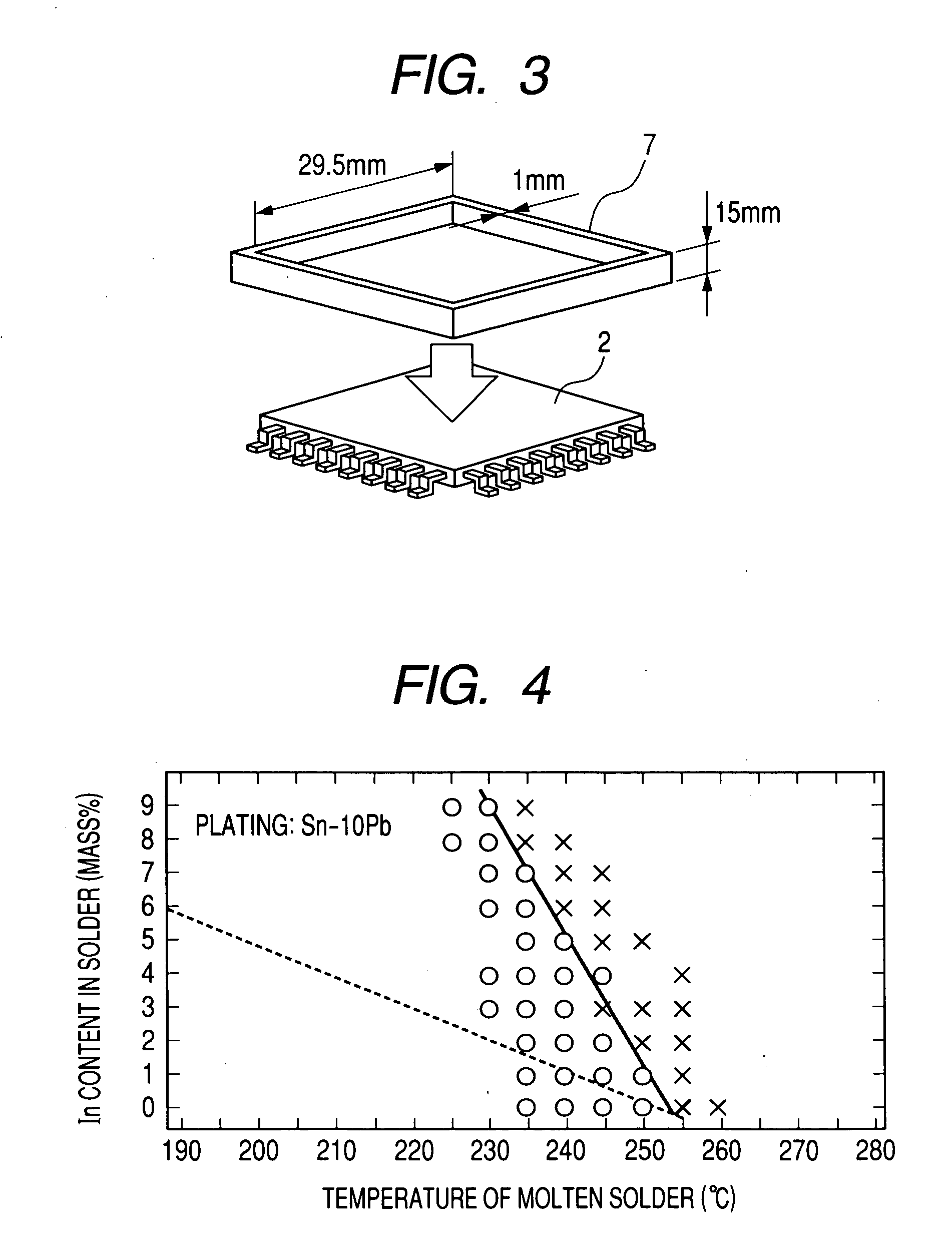
[0050] In a first example, a generally used glass epoxy board 1a was used as a circuit board 1. The glass epoxy board has a thickness of about 1.6 mm, a length of about 350 mm, and a width of about 350 mm. It is provided on its board surface with a copper foil having a thickness of about 18 μm, and has through holes each having an inner diameter of 1 mm and a Cu pad diameter of about 1.6 mm formed at a density of about 0.7 N / cm2.
[0051] A QFP-LSI 2a of 32 mm square was used as a surface mounting pad 2. It has a lead pitch of about 0.5 mm and a lead width of about 0.2 mm and is provided with 208 leads made of 42 alloy subjected to Sn-10 mass % Pb plating.
[0052] Then, the QFP-LSI 2a of 32 mm square was flow soldered to the upper surface of the glass epoxy board 1a by 10 types of In-incorporated solder pastes of Sn-3Ag-0.5Cu-xIn (0≦x≦9, unit: mass %) (details are shown in the following Table 1).
TABLE 1Solder compositionSolidus temperatureLiqiudus temperature(mass %)(° C.)(° C.)Sn—3A...
second example
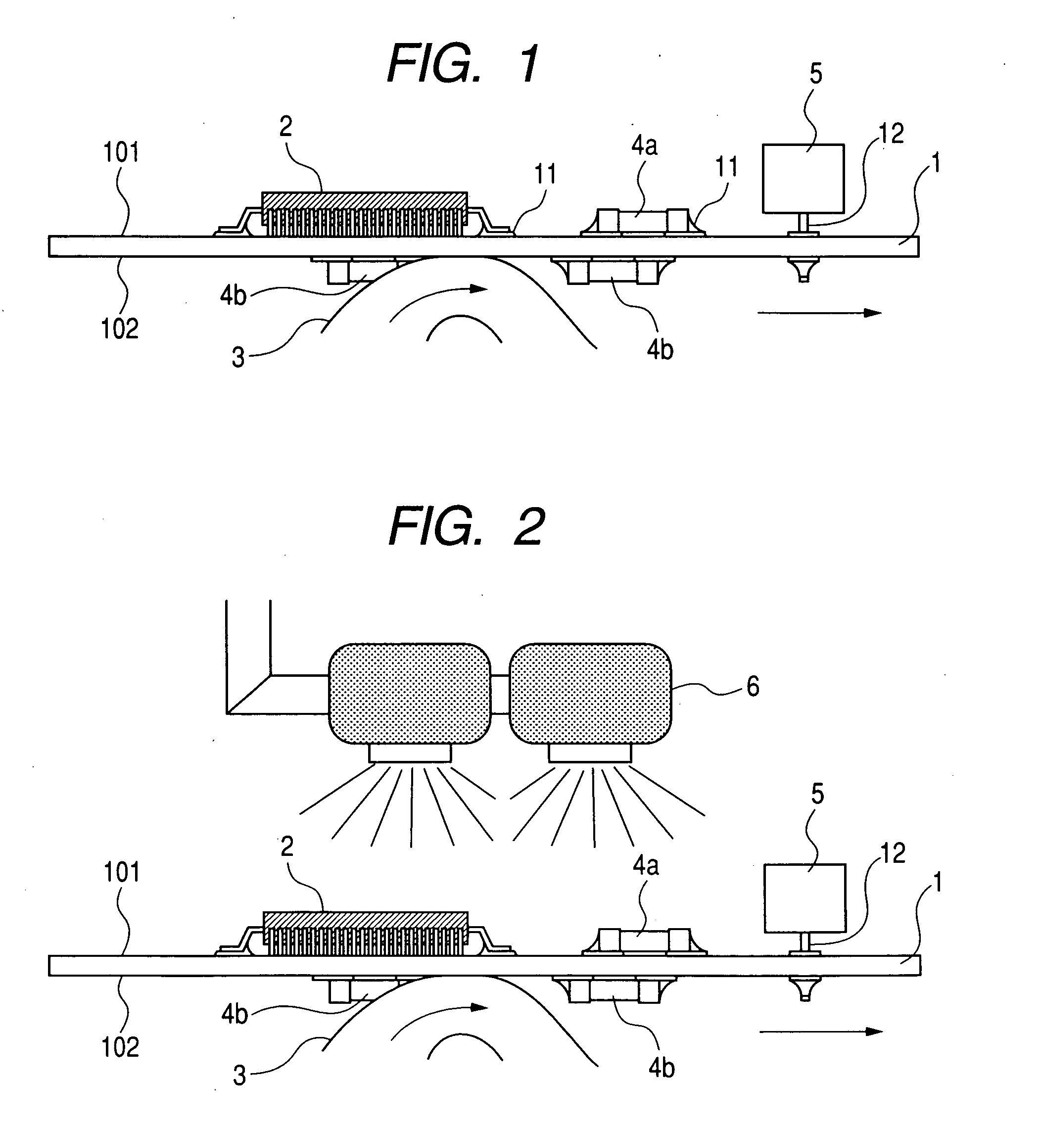
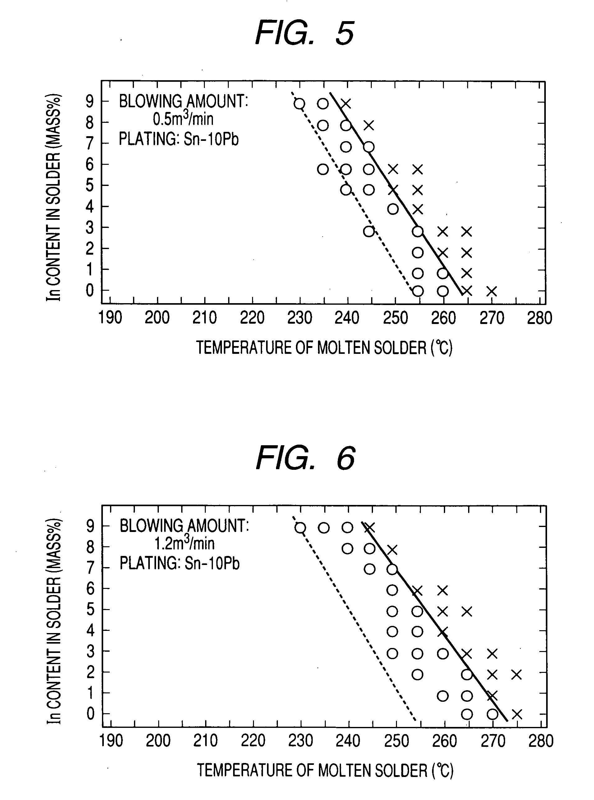
[0064] A second example is different from the first example in that a fluid such as nitrogen was blown to the upper surface 101 of the circuit board 1 for cooling as shown in FIG. 2 at about 20° C. to 50° C. at a flow rate of about 0.5 m3 / min. In FIG. 5, the temperature of the molten solder in the flow soldering bath is indicated on the abscissa and the In content of the solder used for the connection of QFP-LSI is indicated on the coordinate, and conditions causing no breakage is shown by symbol “◯” and the condition causing breakage is shown by symbol “X”. Further, the solid line in FIG. 5 is a line to be considered as a boundary between the conditions causing breakage and the conditions not causing the breakage.
[0065] The results of an experiment in the second example as shown in FIG. 5 confirm that the upper limit of the temperature of the flow molten solder can be increased by about 10° C. or less compared with the first example shown in FIG. 4. Further, the results of the exp...
third example
[0066] In a third example, as shown in FIG. 2, a fluid such as nitrogen at about 20° C. to 50° C. was blown for cooling at a flow rate of about 1.2 m3 / min by a board cooling device 6 in the second example. In FIG. 6, the temperature of the molten solder in the flow soldering bath is indicated on the abscissa and the In content in the solder used for the connection of QFP-LSI is indicated on the abscissa, and the condition not causing breakage is indicated by symbol “◯” and the condition causing the breakage is indicated by the symbol “X”. Further, the solid line in FIG. 6 is a line considered to be a boundary between the conditions causing breakage and the conditions not causing the same.
[0067] The results of the experiment for the third example as shown in FIG. 6 confirm that the upper limit for the allowable melting temperature of the flow solder can be increased by about 15° C. compared with the first example shown in FIG. 4. Further, the results of the experiment shown in FIG. ...
PUM
| Property | Measurement | Unit |
|---|---|---|
| Temperature | aaaaa | aaaaa |
| Temperature | aaaaa | aaaaa |
| Temperature | aaaaa | aaaaa |
Abstract
Description
Claims
Application Information