Printed wiring board design method, program thereof, recording medium storing the program recorded therein, printed wiring board design device using them and cad system

a printed wiring board and design method technology, applied in the field of cad system, can solve the problems of insufficient design device for unnecessary radiation noise reduction of circuit boards, inability to implement sufficient emc design in a limited design time, and increasing the difficulty of emc design

Inactive Publication Date: 2006-10-26
GK BRIDGE 1
View PDF18 Cites 9 Cited by
  • Summary
  • Abstract
  • Description
  • Claims
  • Application Information

AI Technical Summary

Benefits of technology

[0013] A printed wiring board design method pertaining to the invention can also further include the step of: evaluating placement of and wiring for the EC reduction component in the placement and wiring range based on allowances of design values of the items of the EMC design rule and weights set to the items.
[0014] According to a printed wiring board design method pertaining to the invention, since a placement and wiring range for an EMC component is calculated based on the EMC design rule, for example, placement of and wiring for a new bypass capacitor or the like can be implemented and a region satisfying restraint items from the design rule can be clearly displayed as a new input enable region on a CAD scr

Problems solved by technology

Electronic equipment in recent years has advanced the progress of down sizing, high functionality and digitalization, which has entailed increase in unnecessary radiation noise exerting an influence on other electronic equipment of an electromagnetic wave radiated by the electronic equipment of interest, which has increasingly enhanced more and more a necessity for a measure to diminish the unnecessary radiation noise, whereas since there is a relationship of a trade-off between the measure to be taken and down sizing,

Method used


Image

  • Printed wiring board design method, program thereof, recording medium storing the program recorded therein, printed wiring board design device using them and cad system
  • Printed wiring board design method, program thereof, recording medium storing the program recorded therein, printed wiring board design device using them and cad system
  • Printed wiring board design method, program thereof, recording medium storing the program recorded therein, printed wiring board design device using them and cad system

Examples


embodiment

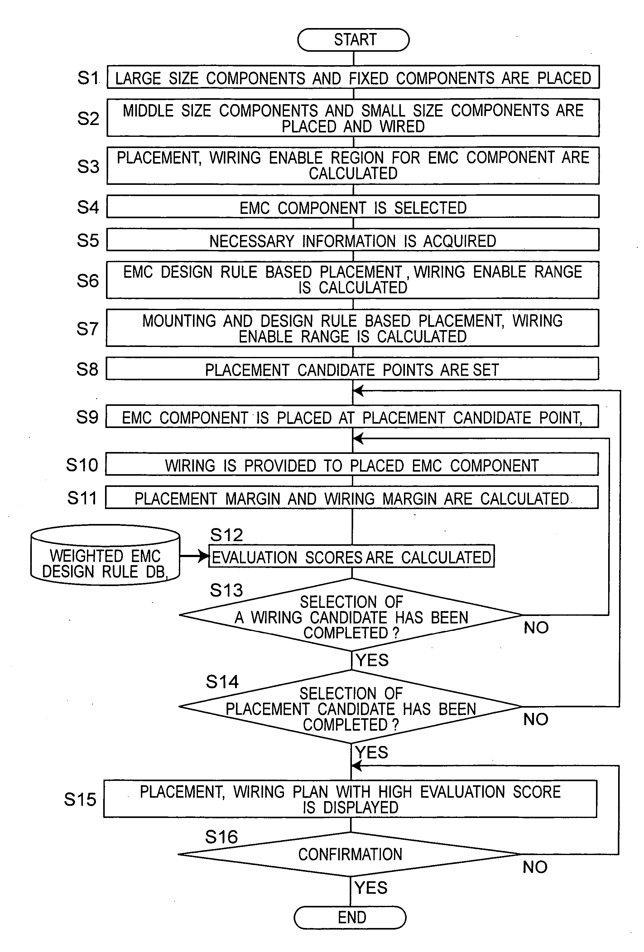
[0045]FIG. 1 is a flowchart of a printed wiring board design method of an embodiment pertaining to the invention and the optimal EMC design can be acquired without dependency on a designer by conducting printed wiring board design, following the flowchart.

[0046] Description will be given of a printed wiring board design method of the embodiment below based on the flowchart of FIG. 1.

[0047] Step S1

[0048] In step S1 of the printed wiring board design method of the embodiment, of large scale ICs, middle scale ICs, connectors (terminals) and components of an IC peripheral circuit, which are extracted based on information on circuit components, placement of the large scale ICs and the like (large size components) occupying a comparative large mounting area and the connectors (terminals), which are fixed components and placement positions of which are determined in advance is determined based on information on circuit wiring and terminal placement

[0049] Step S2

[0050] Then, in step S2, ...


PUM


Abstract

A printed wiring board design method including the steps of designing placement and wiring for circuit components based on circuit information on a mounting surface of the board; excluding a placement region and a wiring region for the circuit components from the mounting surface to thereby calculate a placement and wiring enable region for an EMC component in which the EMC component can be placed and wiring can be laid down; and calculating the placement and wiring range for the EMC component based on an EMC design rule from the calculated placement and wiring enable region for the EMC component, thereby providing a printed wiring board design method in which a placement of and wiring for a new bypass capacitor or the like can be implemented and a region satisfying restraint items from the design rule can be clearly displayed as a new input enable region on a CAD screen.

Description

TECHNICAL FIELD [0001] This invention relates to a CAD system for designing a printed wiring board, a printed wiring board design method, a printed wiring board design device, and a method and device for an EMC design, applicable to the CAD system. BACKGROUND ART [0002] Electronic equipment in recent years has advanced the progress of down sizing, high functionality and digitalization, which has entailed increase in unnecessary radiation noise exerting an influence on other electronic equipment of an electromagnetic wave radiated by the electronic equipment of interest, which has increasingly enhanced more and more a necessity for a measure to diminish the unnecessary radiation noise, whereas since there is a relationship of a trade-off between the measure to be taken and down sizing, EMC design has become technically more and more difficult coping therewith every year. [0003] Various noise reduction designs have been studied: such as high frequency isolation of IC power supply wiri...

Claims


Application Information

Patent Timeline
IPC IPC(8): G06F17/50H05K1/02H05K3/00
CPCG06F17/5072G06F17/5081H05K2201/10689H05K3/0005H05K1/0231G06F30/392G06F30/398
Inventor MIMURA, SHOICHIFUSAYASU, HIROTSUGUIRIKIIN, MIYOKOHAMADA, SEIJI
Owner GK BRIDGE 1
Why Eureka
Try Eureka